Pin configuration, Atmel ata6670 [preliminary – Rainbow Electronics ATA6670 User Manual
Page 3
3
9204C–AUTO–09/11
Atmel ATA6670 [Preliminary]
2.
Pin Configuration
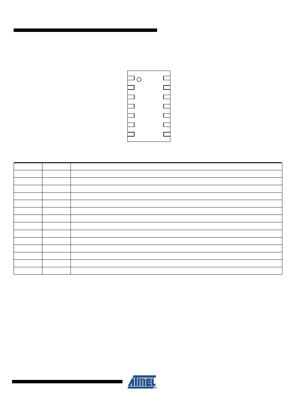
Figure 2-1.
Pinning DFN14
RXD1
EN1
TXD1
RXD2
EN2
WAKE2
TXD2
V
S
1
LIN1
GND1
INH2
V
S
2
Atmel
ATA6670
LIN2
GND2
Table 2-1.
Pin Description
Pin
Symbol
Function
1
RXD1
Receives data output 1 (open drain)
2
EN1
Enables normal mode 1. When the input is open or low, transceiver 1 is in sleep mode.
3
TXD1
Transmits data input 1, active low output (strong pull-down) after a local wake-up request
4
RXD2
Receives data output 2 (open drain)
5
EN2
Enables normal mode 2. When the input is open or low, transceiver 2 is in sleep mode.
6
WAKE2
High voltage input for local wake-up request. If not needed, connect directly to VS2
7
TXD2
Transmits data input 2, active low output (strong pull-down) after a local wake-up request
8
GND2
Ground 2
9
LIN2
LIN bus line 2 input/output
10
VS2
Battery supply 2
11
INH2
VS2- related high-side switch output for controlling an external load, such as a voltage divider
12
GND1
Ground 1
13
LIN1
LIN bus line 1 input/output
14
VS1
Battery supply 1