Atmel ata6670 [preliminary, Electrical characteristics (continued) – Rainbow Electronics ATA6670 User Manual
Page 13
13
9204C–AUTO–09/11
Atmel ATA6670 [Preliminary]
5
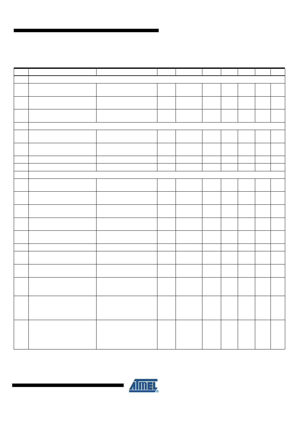
INH 2 Output Pin (Only Available at Transceiver 2)
5.1
High-level voltage
Normal or fail-safe mode
I
INH2
= –15mA
INH2
V
INH2H
V
S2
–
0.75
V
S2
V
A
5.2
Switch-on resistance between
VS2 and INH2
Normal or fail-safe mode
INH2
R
INH2
30
50
Ω
A
5.3
Leakage current
Transceiver 2 in sleep mode
V
INH2
= 0V/27V, V
S2
= 27V
INH2
I
INH2L
–3
+3
µA
A
6
WAKE2 Input Pin (only available at Transceiver 2)
6.1
High-level input voltage
WAKE2
V
WAKE2H
V
S2
–
1V
V
S2
+
0.3V
V
A
6.2
Low-level input voltage
I
WAKE2
= typically –3µA
WAKE2
V
WAKE2L
–1V
V
S2
–
3.3V
V
A
6.3
Wake2 pull-up current
V
S2
< 27V
WAKE2
I
WAKE2
–30
–10
µA
A
6.4
High-level leakage current
V
S2
= 27V, V
WAKE2
= 27V
WAKE2
I
WAKE2
–5
+5
µA
A
7
LIN Bus Driver
7.1
Driver recessive output voltage
R
LOAD
= 500
Ω
/1k
Ω
LIN
V
BUSrec
0.9
×
V
S
V
S
V
A
7.2
Driver dominant voltage
V
BUSdom_DRV_LoSUP
V
VS
= 7V, R
load
= 500
Ω
LIN
V
_LoSUP
1.2
V
A
7.3
Driver dominant voltage
V
BUSdom_DRV_HiSUP
V
VS
= 18V, R
load
= 500
Ω
LIN
V
_HiSUP
2
V
A
7.4
Driver dominant voltage
V
BUSdom_DRV_LoSUP
V
VS
= 7V, R
load
= 1000
Ω
LIN
V
_LoSUP_1k
0.6
V
A
7.5
Driver dominant voltage
V
BUSdom_DRV_HiSUP
V
VS
= 18V, R
load
= 1000
Ω
LIN
V
_HiSUP_1k_
0.8
V
A
7.6
Pull-up resistor to V
S
The serial diode is mandatory
LIN
R
LIN
20
30
47
k
Ω
A
7.7
Voltage drop at the serial diodes
In pull-up path with R
slave
I
SerDiode
= 10mA
LIN
V
SerDiode
0.4
1.0
V
D
7.8
LIN current limitation
V
BUS
= V
BAT_max
LIN
I
BUS_LIM
40
120
200
mA
A
7.9
Input leakage current at the
receiver, including pull-up
resistor as specified
Input leakage current
driver off
V
BUS
= 0V, V
S
= 12V
LIN
I
BUS_PAS_dom
–1
mA
A
7.10 Leakage current LIN recessive
Driver off
8V < V
BAT
< 18V
8V < V
BUS
< 18V
V
BUS
≥
V
BAT
LIN
I
BUS_PAS_rec
10
20
µA
A
7.11
Leakage current at ground loss;
control unit disconnected from
ground; loss of local ground must
not affect communication in the
residual network
GND
Device
= V
S
V
BAT
=12V
0V < V
BUS
< 18V
LIN
I
BUS_NO_Gnd
–10
+0.5
+10
µA
A
6.
Electrical Characteristics (Continued)
5V < V
S
< 27V, T
j
= –40°C to +150°C; the values below are valid for each of the two nearly identical integrated LIN transceivers unless
otherwise specified.
No.
Parameters
Test Conditions
Pin
Symbol
Min.
Typ.
Max.
Unit
Type*
*) Type means: A = 100% tested, B = 100% correlation tested, C = Characterized on samples, D = Design parameter