Ata6827 [preliminary, Pin configuration – Rainbow Electronics ATA6827 User Manual
Page 3
3
4912C–AUTO–10/06
ATA6827 [Preliminary]
2.
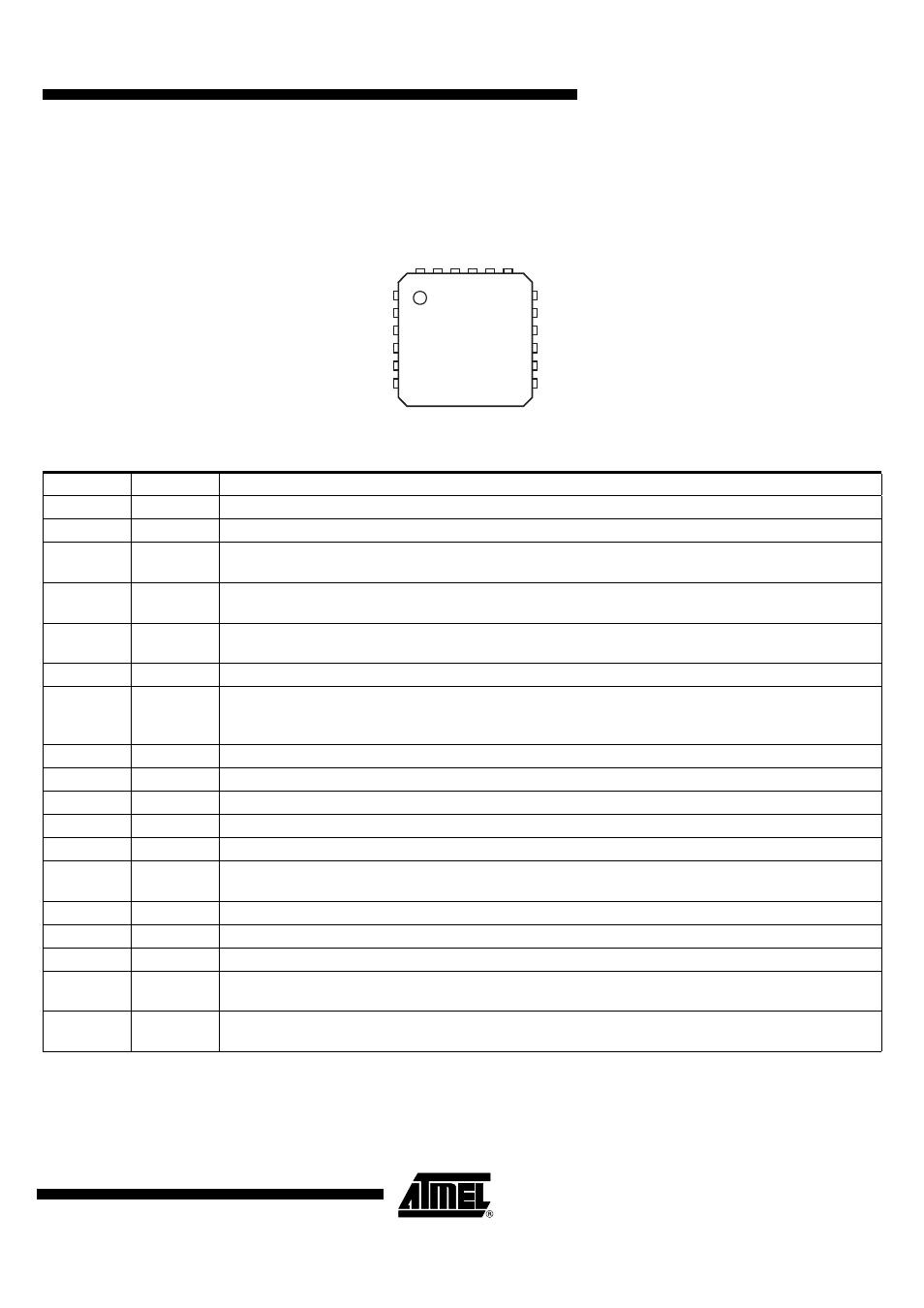
Pin Configuration
Figure 2-1.
Pinning QFN18
OUT3S
OUT3
CS
DI
CLK
GND
OUT2
VS
VS
VCC
INH
DO
PGND3
PGND1
OUT1S
OUT1F
PGND2
OUT2S
1
2
3
4
5
6
12
11
10
9
8
7
18 17 16 15
13
14
Table 2-1.
Pin Description
Pin
Symbol
Function
1
OUT3S
Sense OUT3, internal connected to pin 2 via lead
2
OUT3
Half-bridge output 3
3
CS
Chip select input; 5-V CMOS logic level input with internal pull up;
low = serial communication is enabled, high = disabled
4
DI
Serial data input; 5-V CMOS logic level input with internal pull down; receives serial data from the control
device; DI expects a 16-bit control word with LSB being transferred first
5
CLK
Serial clock input; 5-V CMOS logic level input with internal pull down;
controls serial data input interface and internal shift register (f
max
= 2 MHz)
6
GND
Ground; reference potential
7
DO
Serial data output; 5-V CMOS logic level tri-state output for output (status) register data; sends 16-bit
status information to the microcontroller (LSB is transferred first); output will remain tri-stated unless
device is selected by CS = low, therefore, several ICs can operate on one data output line only.
8
INH
Inhibit input; 5-V logic input with internal pull down; low = standby, high = normal operation
9
VCC
Logic supply voltage (5 V)
10
VS
Power supply for output stages OUT1, OUT2 and OUT3, internal supply
11
VS
Power supply for output stages OUT1, OUT2 and OUT3, internal supply
12
OUT2
Half-bridge output 2
13
OUT2S
Sense OUT2, internal connected to pin 12 via bond; OUT2 controlled loads have to be connected to pin
12 OUT2F
14
PGND2
Power Ground OUT2
15
OUT1F
Half-bridge output 1
16
OUT1S
Sense OUT1, internal connected to pin 15 via lead
17
PGND1
PGND3
Power Ground OUT1 and OUT3
18
PGND1
PGND3
Power Ground OUT1 and OUT3