Absolute maximum ratings, Recommended dc operating conditions, Dc electrical characteristics – Rainbow Electronics DS1858 User Manual
Page 2
DS1858
Dual Temperature-Controlled Resistors with
Three Monitors
2
_____________________________________________________________________
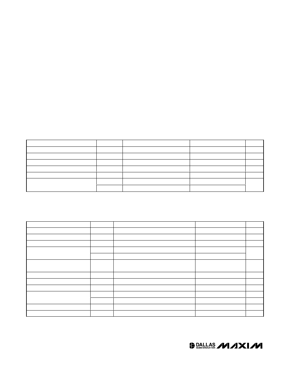
PARAMETER
SYMBOL
CONDITIONS
MIN
TYP
MAX
UNITS
Supply Voltage
V
CC
(Note 1)
3.0
5.5
V
Input Logic 1 (SDA, SCL, WPEN)
V
IH
(Note 2)
0.7 x Vcc
V
CC
+ 0.3
V
Input Logic 0 (SDA, SCL, WPEN)
V
IL
(Note 2)
-0.3
0.3 x V
CC
V
Resistor Inputs (L0, L1, H0, H1)
-0.3
V
CC
+ 0.3
V
Resistor Current
I
RES
-3
+3
mA
V
IH
Input logic 1
1.5
Input Logic Levels (IN1, IN2)
V
IL
Input logic 0
0.9
V
ABSOLUTE MAXIMUM RATINGS
Stresses beyond those listed under “Absolute Maximum Ratings” may cause permanent damage to the device. These are stress ratings only, and functional
operation of the device at these or any other conditions beyond those indicated in the operational sections of the specifications is not implied. Exposure to
absolute maximum rating conditions for extended periods may affect device reliability.
Voltage on V
CC
Relative to Ground.......................-0.5V to +6.0V
Voltage on Inputs Relative
to Ground* ................................................-0.5V to V
CC
+ 0.5V
Voltage on Resistor Inputs Relative
to Ground* ................................................-0.5V to V
CC
+ 0.5V
Current into Resistors............................................................5mA
Operating Temperature Range ...........................-40°C to +95°C
Programming Temperature Range .........................0°C to +70°C
Storage Temperature Range .............................-55°C to +125°C
Soldering Temperature .......................................See IPC/JEDEC
RECOMMENDED DC OPERATING CONDITIONS
(T
A
= -40°C to +95°C, unless otherwise noted.)
PARAMETER
SYMBOL
CONDITIONS
MIN
TYP
MAX
UNITS
Supply Current
I
CC
(Note 3)
1
2
mA
Input Leakage
I
IL
-1
+1
µA
Input Current each I/O Pin
0.4 x V
CC
< V
I/O
< 0.9 x V
CC
-10
+10
µA
V
OL1
3mA sink current
0
0.4
Low-Level Output Voltage (SDA)
V
OL2
6mA sink current
0
0.6
V
Full-Scale Input (MON1, MON2,
MON3)
(Note 4)
2.4875
2.5
2.5125
V
Full-Scale V
CC
Monitor
(Note 5)
6.5208
6.5536
6.5864
V
I/O Capacitance
C
I/O
10
pF
WPEN Pullup
R
WPEN
40
65
100
k
Ω
V
OL1
3mA sink current
0
0.4
V
OUT1, OUT2 Voltage
V
OL2
6mA sink current
0
0.6
V
Digital Power-On Reset
POD
1.0
2.2
V
Analog Power-On Reset
POA
2.0
2.6
V
DC ELECTRICAL CHARACTERISTICS
(V
CC
= 3.0V to 5.5V, T
A
= -40°C to +95°C, unless otherwise noted.)
*Not to exceed 6.0V.