Table 01h (continued), Table 02h, Table 03h – Rainbow Electronics DS1858 User Manual
Page 17
DS1858
Dual Temperature-Controlled Resistors with
Three Monitors
____________________________________________________________________
17
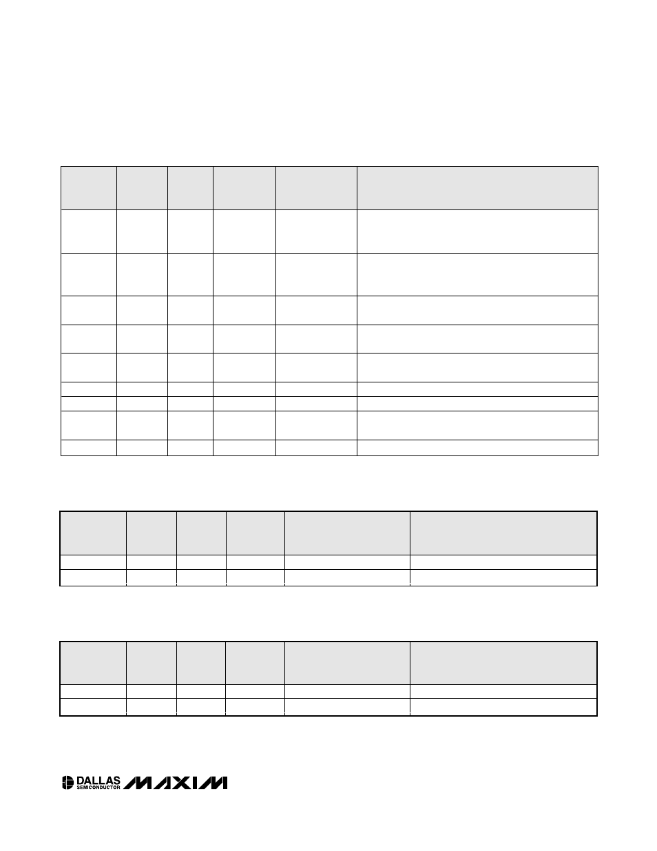
MEMORY
LOCATION
(hex)
EEPROM/
SRAM
R/W
DEFAULT
SETTING
(hex)
NAME OF
LOCATION
FUNCTION
5
—
—
0
ADEN
Controls if the device responds to one or two device
addresses (see the Memory Description section and
Table 5).
4
—
—
0
ADFIX
Controls the means by which Main and Auxiliary Device
addresses are set (see the Memory Description section
and Table 5).
3
—
—
0
APEN
Controls auxiliary write protect. See the Memory
Description section.
2
—
—
0
MPEN
Controls main write protect. See the Memory Description
section.
1
—
—
0
INV1
Configures buffer 1 with OUT1 = MINT +
(INV1 [XOR] IN1).
0
—
—
0
INV2
Configures buffer 2 with OUT2 = INV2 [XOR] IN2.
8A to 8B
EEPROM
—
00
Reserved
8C
EEPROM
R/W
A2
Device address
Contains Main Device address if the bit ADFIX = 1. If
ADFIX = 0, then address A2h is used.
8D to 8F
EEPROM
—
—
Reserved
—
Table 01h (continued)
MEMORY
LOCATION
(hex)
EEPROM/
SRAM
R/W
DEFAULT
SETTING
(hex)
NAME OF LOCATION
FUNCTION
80 to C7
EEPROM
R/W
FF
Resistor 0 Temp LUT
Look-up table for Resistor 0.
F0 to FF
EEPROM
R
FF
Reserved
—
Table 02h
MEMORY
LOCATION
(hex)
EEPROM/
SRAM
R/W
DEFAULT
SETTING
(hex)
NAME OF LOCATION
FUNCTION
80 to C7
EEPROM
R/W
FF
Resistor 1 Temp LUT
Look-up table for Resistor 1.
F0 to FF
EEPROM
R
FF
Reserved
Table 03h