Ac timing characteristics – 5v operation, At6000(lv) series – Rainbow Electronics AT6010LV User Manual
Page 19
AT6000(LV) Series
19
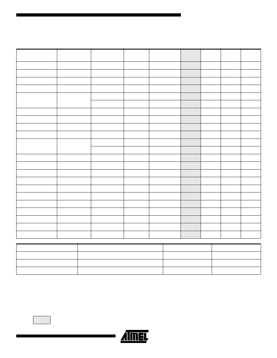
AC Timing Characteristics – 5V Operation
Notes:
1. TTL buffer delays are measured from a V
IH
of 1.5V at the pad to the internal V
IH
at A. The input buffer load is constant.
2. CMOS buffer delays are measured from a V
IH
of 1/2 V
CC
at the apd to the internal V
IH
at A. The input buffer load is constant.
3. Buffer delay is to a pad voltage of 1.5V with one output switching.
4. Max specifications are the average of mas t
PDLH
and t
PDHL
.
5. Parameter based on characterization and simulation; not tested in production
6. Exact power calculation is available in an Atmel application note.
7. Load Definition: 1 = Load of one A or B input; 2 = Load of one L input; 3 = Constant Load; 4 = Tester Load of 50 pF.
Delays are based on fixed load. Loads for each type of device are described in the notes. Delays are in nanoseconds.
Worst case: V
CC
= 4.75V to 5.25V. Temperature = 0
°
C to 70
°
C.
Cell Function
Parameter
From
To
Load
Definition
-1
-2
-4
Units
Wire
t
PD
(max)
A, B, L
A, B
1
0.8
1.2
1.8
ns
NAND
t
PD
(max)
A, B, L
B
1
1.6
2.2
3.2
ns
XOR
t
PD
(max)
A, B, L
A
1
1.8
2.4
4.0
ns
AND
t
PD
(max)
A, B, L
B
1
1.7
2.2
3.2
ns
MUX
t
PD
(max)
A, B
A
1
1.7
2.3
4.0
ns
L
A
1
2.1
3.0
4.9
ns
D-Flip-flop
t
setup
(min)
A, B, L
CLK
-
1.5
2.0
3.0
ns
D-Flip-flop
t
hold
(min)
CLK
A, B, L
-
0
0
0
ns
D-Flip-flop
t
PD
(max)
CLK
A
1
1.5
2.0
3.0
ns
Bus Driver
t
PD
(max)
A
L
2
2.0
2.6
4.0
ns
Repeater
t
PD
(max)
L, E
E
3
1.3
1.6
2.3
ns
L, E
L
2
1.7
2.1
3.0
ns
Column Clock
t
PD
(max)
GCLK, A, ES
CLK
3
1.8
2.4
3.0
ns
Column Reset
t
PD
(max)
GRES, A, EN
RES
3
1.8
2.4
3.0
ns
Clock Buffer
t
PD
(max)
CLOCK PIN
GCLK
-
1.6
2.0
2.9
ns
Reset Buffer
t
PD
(max)
RESET PIN
GRES
-
1.5
1.9
2.8
ns
TTL Input
t
PD
(max)
I/O
A
3
1.0
1.2
1.5
ns
CMOS Input
t
PD
(max)
I/O
A
3
1.3
1.4
2.3
ns
Fast Output
t
PD
(max)
A
I/O PIN
4
3.3
3.5
6.0
ns
Slow Output
t
PD
(max)
A
I/O PIN
4
7.5
8.0
12.0
ns
Output Disable
t
PXZ
(max)
L
I/O PIN
4
3.1
3.3
5.5
ns
Fast Enable
t
PXZ
(max)
L
I/O PIN
4
3.8
4.0
6.5
ns
Slow Enable
t
PXZ
(max)
L
I/O PIN
4
8.2
8.5
12.5
ns
Device
Cell Types
Outputs
I
CC
(max)
Cell
Wire, XWire, Half-adder, Flip-flop
A, B
4.5 µA/MHz
Bus
Wire, XWire, Half-adder, Flip-flop, Repeater
L
2.5 µA/MHz
Column Clock
Column Clock Driver
CLK
40 µA/MHz
= Preliminary Information