Rainbow Electronics ADC12048 User Manual
Page 7
Notes on Specifications
(Continued)
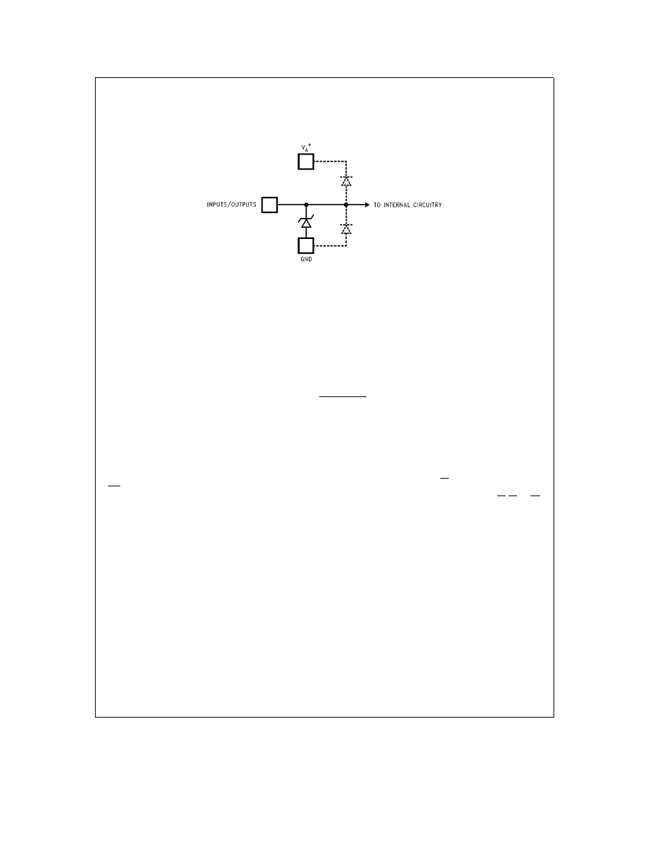
Note 6
Each input and output is protected by a nominal 6 5V breakdown voltage zener diode to GND as shown below input voltage magnitude up to 0 3V above
V
A
a
or 0 3V below GND will not damage the ADC12048 There are parasitic diodes that exist between the inputs and the power supply rails and errors in the A D
conversion can occur if these diodes are forward biased by more than 50 mV As an example if V
A
a
is 4 50 V
DC
full-scale input voltage must be
s
4 55 V
DC
to
ensure accurate conversions
TL H 12387 – 4
Note 7
V
A
a
and V
D
a
must be connected together to the same power supply voltage and bypassed with separate capacitors at each V
a
pin to assure
conversion comparison accuracy Refer to the Power Supply Considerations section for a detailed discussion
Note 8
Accuracy is guaranteed when operating at f
CLK
e
12 MHz
Note 9
With the test condition for V
REF
(V
REF
a
b
V
REF
b
) given as
a
4 096V the 12-bit LSB is 1 000 mV
Note 10
Typicals are at T
A
e
25 C and represent most likely parametric norm
Note 11
Limits are guaranteed to National’s AOQL (Average Outgoing Quality Level)
Note 12
Positive integral linearity error is defined as the deviation of the analog value expressed in LSBs from the straight line that passes through positive full-
scale and zero For negative integral linearity error the straight line passes through negative full-scale and zero
Note 13
Zero error is a measure of the deviation from the mid-scale voltage (a code of zero) expressed in LSB It is the average value of the code transitions
between
b
1 to 0 and 0 to
a
1 (see
Figure 6 )
Note 14
The DC common-mode error is measured with both inputs shorted together and driven from 0V to 5V The measured value is referred to the resulting
output value when the inputs are driven with a 2 5V input
Note 15
Power Supply Sensitivity is measured after an Auto-Zero and Auto Calibration cycle has been completed with V
A
a
and V
D
a
at the specified extremes
Note 16
V
REFCM
(Reference Voltage Common Mode Range) is defined as
V
REF
a
a
V
REF
b
2
J
Note 17
The ADC12048’s self-calibration technique ensures linearity and offset errors as specified but noise inherent in the self-calibration process will result in a
repeatability uncertainly of
g
0 20 LSB
Note 18
Total Unadjusted Error (TUE) includes offset full scale linearity and MUX errors
Note 19
The ADC12048 parts used to gather the information for these curves were auto-calibrated prior to taking the measurements at each test condition The
auto-calibration cycle cancels any first order drifts due to test conditions However each measurement has a repeatability uncertainty error of 0 2 LSB See Note
17
Note 20
This is a DC average current drawn by the reference input with a full-scale sinewave input The ADC12048 is continuously converting with a throughput
rate of 206 kHz
Note 21
These typical curves were measured during continuous conversions with a positive half-scale DC input A 240 ns RD pulse was applied 25 ns after the
RDY signal went low The data bus lines were loaded with 2 HC family CMOS inputs (C
L
E
20 pF)
Note 22
Any other values placed in the command field are meaningless However if a code of 101 or 110 is placed in the command field and the CS RD and WR
go low at the same time the ADC12048 will enter a test mode These test modes are only to be used by the manufacturer of this device A hardware power-off and
power-on reset must be done to get out of these test modes
7