Pin description – Rainbow Electronics ADC12048 User Manual
Page 20
Pin Description
PLCC Pkg
PQFP Pkg
Pin Name
Description
Pin Number
Pin Number
6
44
CH0
The eight analog inputs to the Multiplexer Active channels are selected based on the contents of bits b3–b0 of the
7
1
CH1
Configuration register Refer to section titled MUX for more details
8
2
CH2
9
3
CH3
15
9
CH4
16
10
CH5
17
11
CH6
18
12
CH7
14
8
COM
This pin is another analog input pin used as a pseudo ground when the multiplexer is configured in single-ended mode
13
7
V
REF
a
Positive reference input The operating voltage range for this input is 1V
s
V
REF
a
s
V
A
a
(see
Figures 3 and 4 ) This
pin should be bypassed to AGND at least with a parallel combination of a 10 mF and a 0 1 mF (ceramic) capacitors The
capacitors should be placed as close to the part as possible
12
6
V
REF
b
Negative reference input The operating voltage range for this input is 0V
s
V
REF
b
s
V
REF
a
b
1 (see
Figures 3 and
4 ) This pin should be bypassed to AGND at least with a parallel combination of a 10 mF and a 0 1 mF (ceramic)
capacitor The capacitors should be placed as close to the part as possible
19
13
MUX OUT
b
The inverting (negative) and non-inverting (positive) outputs of the multiplexer
21
15
MUX OUT
a
The analog inputs to the MUX selected by bits b3–b0 of the Configuration register appear at these pins
20
14
ADCIN
b
ADC inputs The inverting (negative) and non-inverting (positive) inputs into the ADC
22
16
ADCIN
a
24
18
WMODE
The logic state of this pin at power-up determines which edge of the write signal (WR) will latch in data from the data
bus If tied low the ADC12048 will latch in data on the rising edge of the WR signal If tied to a logic high data will he
latched in on the falling edge of the WR signal The state of this pin should not be changed after power-up
25
19
SYNC
The SYNC pin can be programmed as an input or an output The Configuration register’s bit b8 controls the function of
this pin When programmed as an input pin (b8
e
1) a rising edge on this pin causes the ADC’s sample-and-hold to
hold the analog input signal and begin conversion When programmed as an output pin (b8
e
0) the SYNC pin goes
high when a conversion begins and returns low when completed
26–31
20–25
D0–D5
13-bit Data bus of the ADC12048 D12 is the most significant bit and D0 is the least significant The BW (bus width) bit of
34–40
29–34
D6–D12
the Configuration register (b12) selects between an 8-bit or 13-bit data bus width When the BW bit is cleared (BW
e
0)
D7–D0 are active and D12–D8 are always in TRI-STATE When the BW bit is set (BW
e
1) D12–D0 are active
43
37
CLK
The clock input pin used to drive the ADC12048 The operating range is 0 05 MHz to 12 MHz
44
38
WR
WR is the active low WRITE control input pin A logic low on this pin and the CS will enable the input buffers of the data
pins D12–D0 The signal at this pin is used by the ADC12048 to latch in data on D12–D0 The sense of the WMODE pin
at power-up will determine which edge of the WR signal the ADC12048 will latch in data See WMODE pin description
1
39
RD
RD is the active low read control input pin A logic low on this pin and CS will enable the active output buffers to drive the
data bus
2
40
CS
CS is the active low Chip Select input pin Used in conjunction with the WR and RD signals to control the active data bus
input output buffers of the data bus
3
41
RDY
RDY is an active low output pin The signal at this pin indicates when a requested function has begun or ended Refer to
section Functional Description and the digital timing diagrams for more detail
4
42
STDBY
This is the standby active low output pin This pin is low when the ADC12048 is in the standby mode and high when the
ADC12048 is out of the standby mode or has been requested to leave the standby mode
10
4
V
A
a
Analog supply input pin The device operating supply voltage range is
a
5V
g
10% Accuracy is guaranteed only if the
V
A
a
and V
D
a
are connected to the same potential This pin should be bypassed to AGND with a parallel combination
of a 10 mF and a 0 1 mF (ceramic) capacitor The capacitors should be placed as close to the supply pins of the part as
possible
11
5
AGND
Analog ground pin This is the device’s analog supply ground connection It should be connected through a low
resistance and low inductance ground return to the system power supply
32 and 41
26 and 35
V
D
a
Digital supply input pins The device operating supply voltage range is
a
5V
g
10% Accuracy is guaranteed only if the
V
A
a
and V
D
a
are connected to the same potential This pin should be bypassed to DGND with a parallel combination
of a 10 mF and a 0 1 mF (ceramic) capacitor The capacitors should be placed as close to the supply pins of the part as
possible
33 and 42
27 and 36
DGND
Digital ground pin This is the device’s digital supply ground connection It should be connected through a low resistance
and low inductance ground return to the system power supply
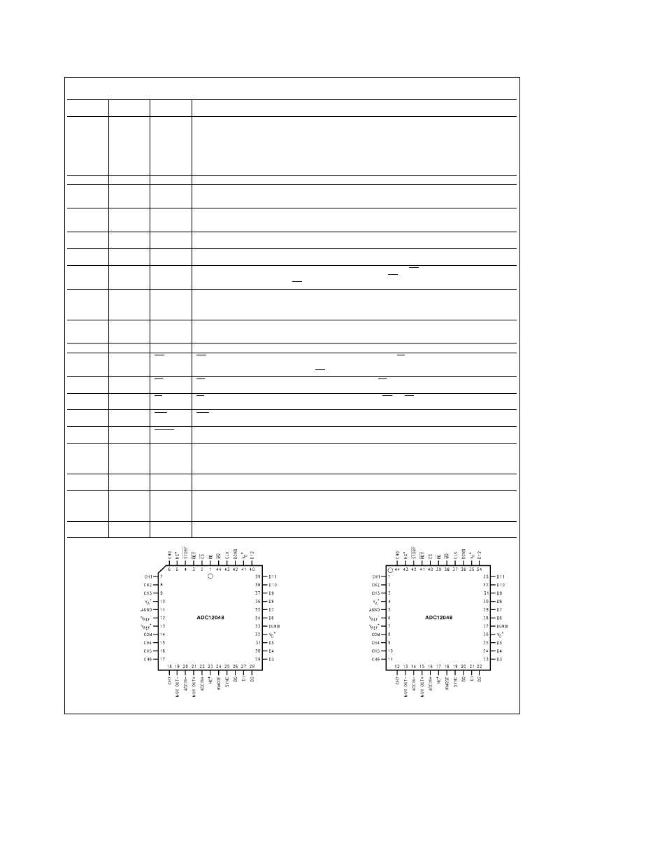
TL H 12387 – 34
TL H 12387 – 35
44-Pin
PLCC Package
Order Number
ADC12048CIV
See NS Package
Number V44A
NC
e
No Connection
These pins maybe
grounded
44-Pin
PQFP Package
Order Number
ADC12048CIVF
See NS Package
Number VGZ44A
20