Analog application information – Rainbow Electronics ADC12048 User Manual
Page 27
Analog Application Information
(Continued)
TL H 12387 – 38
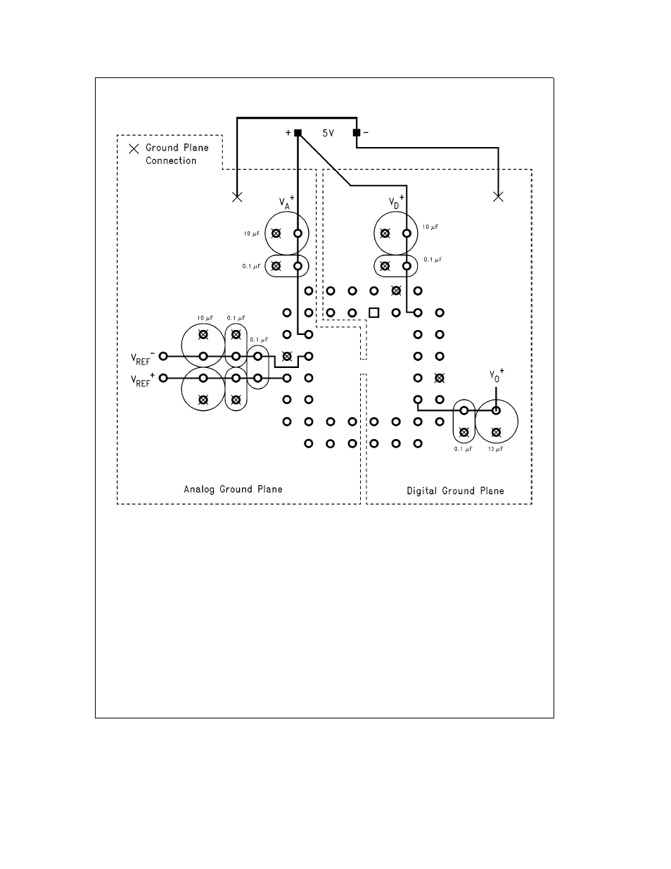
FIGURE 10 Top View of Printed Circuit Board for a 44-Pin PLCC ADC12048
When measuring AC input signals any crosstalk between
analog input output lines and the reference lines (CH0 –
CH7 MUXOUT
g
ADC IN
g
V
REF
g
) should be minimized
Crosstalk is minimized by reducing any stray capacitance
between the lines This can be done by increasing the clear-
ance between traces keeping the traces as short as possi-
ble shielding traces from each other by placing them on
different sides of the AGND plane or running AGND traces
between them
Figure 10
also shows the reference input bypass capacitors
Here the reference inputs are considered to be differential
The performance improves by having a 0 1 mF capacitor
between the V
REF
a
and V
REF
b
and by bypassing in a
manner similar to that described for the supply pins When a
single ended reference is used V
REF
b
is connected to
AGND and only two capacitors are used between V
REF
a
and V
REF
b
(0 1 mF a 10 mF) It is recommended to directly
connect the AGND side of these capacitors to the V
REF
b
instead of connecting V
REF
b
and the ground sides of the
capacitors separately to the ground planes This provides a
significantly lower-impedance connection when using sur-
face mount technology
27