Register bit description – Rainbow Electronics ADC12048 User Manual
Page 21
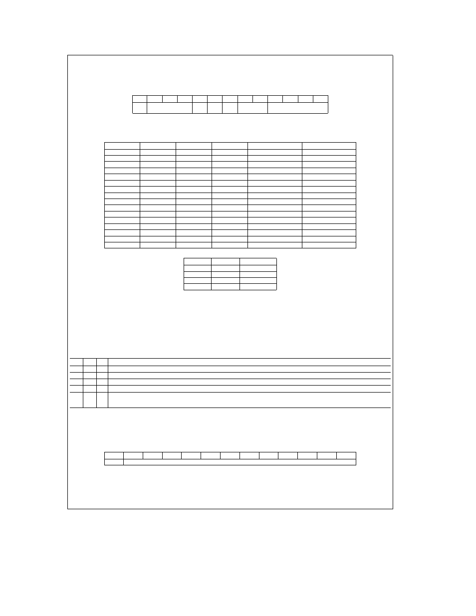
Register Bit Description
CONFIGURATION REGISTER (Write Only)
This is a 13-bit write-only register that is used to program the functionality of the ADC12048 All data written to the ADC12048 will always go to this register only
The contents of this register cannot be read
MSB
LSB
b
12
b
11
b
10
b
9
b
8
b
7
b
6
b
5
b
4
b
3
b
2
b
1
b
0
BW
COMMAND
SYNC
HB
SE
ACQ TIME
MUX ADDRESS
FIELD
Power on State
0100Hex
b
3
–b
0
The MUX ADDRESS bits configure the analog input MUX They select which input channels of the MUX will connect to the MUXOUT
a
and MUXOUT
b
pins (Refer to the MUX section for more details on the MUX ) Power-up value is 0000
TABLE I MUX Channel Assignment
b
3
b
2
b
1
b
0
MUXOUT
a
MUXOUT
b
0
0
0
0
CH0
CH1
0
0
0
1
CH1
CH0
0
0
1
0
CH2
CH3
0
0
1
1
CH3
CH2
0
1
0
0
CH4
CH5
0
1
0
1
CH5
CH4
0
1
1
0
CH6
CH7
0
1
1
1
CH7
CH6
1
0
0
0
CH0
COM
1
0
0
1
CH1
COM
1
0
1
0
CH2
COM
1
0
1
1
CH3
COM
1
1
0
0
CH4
COM
1
1
0
1
CH5
COM
1
1
1
0
CH6
COM
1
1
1
1
CH7
COM
b
5
–b
4
The ACQ TIME bits select one of four possible acquistion times in SYNC-OUT mode (Refer to Selectable Acquisition Time section )
b
5
b
4
Clocks
0
0
9
0
1
15
1
0
47
1
1
79
b
6
When the Single-Ended bit (SE bit) is set conversion results will be limited to positive values only and any negative conversion results will appear as a code of
zero in the Data register The SE bit is cleared at power-up
b
7
The High Byte bit (HB) is meaningful only in 8-bit mode (BW bit b
12
e
‘‘0’’) and is a don’t care condition in 13-bit mode (BW bit b
12
e
‘‘1’’) This bit is used to
access the upper byte of the Configuration Register in 8-bit mode When this bit is set and bit b
12
e
0 the next byte written to the ADC12048 will program the
upper byte of the Configuration register The HB bit will automatically be cleared when data is written to the upper byte of the Configuration register allowing the
lower byte to be accessed with the next write The HB bit is cleared at power-up
b
8
The SYNC bit When the SYNC bit is set the SYNC pin is programmed as an input and the converter is in synchronous mode In this mode a rising edge on the
SYNC pin causes the ADC to hold the input signal and begin a conversion When b
15
cleared the SYNC pin is programmed as an output and the converter is in an
asynchronous mode In this mode the signal at the SYNC pin indicates the status of the converter The SYNC pin is high when a conversion is taking place The
SYNC bit is set at power-up
b
11
–b
9
The command field These bits select the mode of operation of the ADC12048 Power-up value is 000 (See Note 22)
b
11
b
10
b
9
Command
0
0
0
Standby command This puts the ADC in a low power consumption mode
0
0
1
Ful-Cal command This will cause the ADC to perform a self-calibrating cycle that will correct linearity and zero errors
0
1
0
Auto-zero command This will cause the ADC to perform an auto-zero cycle that corrects offset errors
0
1
1
Reset command This puts the ADC in an idle mode
1
0
0
Start command This will put the converter in a start mode preparing it to perform a conversion If in asynchronous mode (b
8
e
‘‘0’’) conversions
will immediately begin after the programmed acquisition time has ended In synchronous mode (b
8
e
‘‘1’’) conversions will begin after a rising
edge appears on the SYNC pin
b
12
This is the Bus Width (BW) bit When this bit is cleared the ADC12048 is configured to interface with an 8-bit data bus data pins D
7
–D
0
are active and pins
D
12
–D
9
are in TRI-STATE When the BW bit is set the ADC12048 is configured to interface with a 16-bit data bus and data pins D
13
–D
0
are all active The BW bit
is cleared at power-up
DATA REGISTER (Read Only)
This is a 13-bit read only register that holds the 12-bit
a
sign conversion result in two’s compliment form All reads performed from the ADC12048 will place the
contents of this register on the data bus When reading the data register in 8-bit mode the sign bit is extended
MSB
LSB
b
12
b
11
b
10
b
9
b
8
b
7
b
6
b
5
b
4
b
3
b
2
b
1
b
0
sign
Conversion Data
Power on State
0000Hex
b
11
–b
0
b
11
is the most significant bit and b
0
is the least significant bit of the conversion result
b
12
This bit contains the sign of the conversion result 0 for positive results and 1 for negative
21