Chip information, Pin configuration – Rainbow Electronics MAX8709 User Manual
Page 22
MAX8709
High-Efficiency CCFL Backlight
Controller with SMBus Interface
22
______________________________________________________________________________________
3)
Route high-speed switching nodes away from sen-
sitive analog areas (CCI, CCV, REF, V
FB
, I
FB
, I
SEC
,
ILIM). Make all pin-strap control input connections
(ILIM, etc.) to analog ground or V
CC
rather than
power ground or V
DD
.
4)
Mount the decoupling capacitor from V
CC
to GND
as close as possible to the IC with dedicated
traces that are not shared with other signal paths.
5)
The current-sense paths for LX1 and LX2 to GND
must be made using Kelvin-sense connections to
guarantee the current-limit accuracy. With 8-pin
SO MOSFETs, this is best done by routing power
to the MOSFETs from outside using the top copper
layer, while connecting GND and LX inside (under-
neath) the 8-pin SO package.
6)
Ensure the feedback connections are short and
direct. To the extent possible, IFB, VFB, and ISEC
connections should be far away from the high-volt-
age traces and the transformer.
7)
To the extent possible, high-voltage trace clear-
ance on the transformer’s secondary should be
widely separated. The high-voltage traces should
also be separated from adjacent ground planes to
prevent lossy capacitive coupling.
8)
The traces to the capacitive voltage-divider on the
transformer’s secondary need to be widely sepa-
rated to prevent arcing. Moving these traces to
opposite sides of the board can be beneficial in
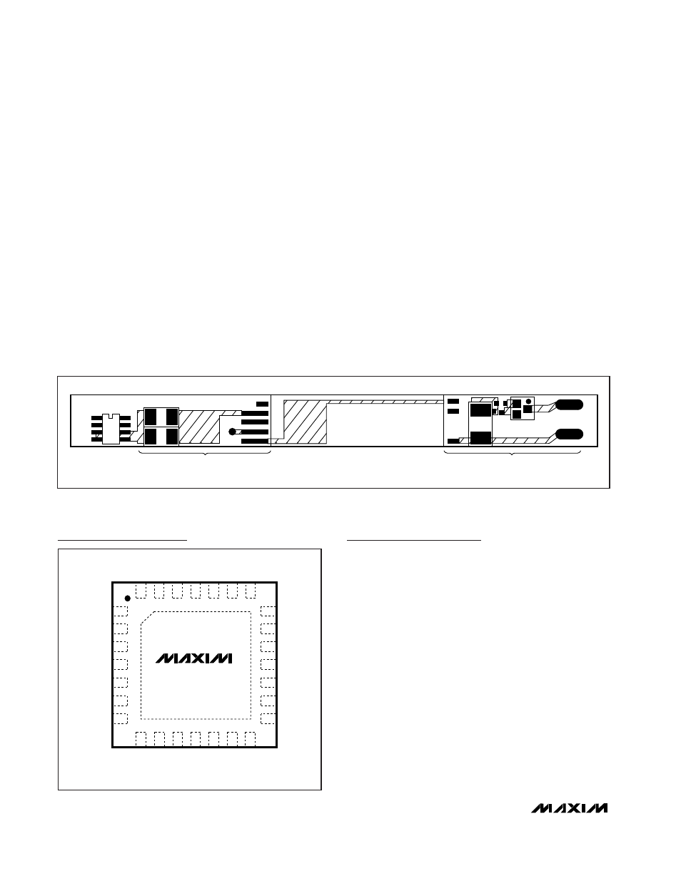
some cases (see Figure 10).
NOTE: DUAL MOSFET N2 IS MOUNTED ON THE BOTTOM SIDE OF THE PC BOARD DIRECTLY UNDER N1.
HIGH-CURRENT PRIMARY CONNECTION
HIGH-VOLTAGE SECONDARY CONNECTION
LAMP
N1
N2
T1
C4
C2
D1
R2
C3
Figure 10. High-Voltage Components Layout Example
Chip Information
TRANSISTOR COUNT: 7116
PROCESS: BiCMOS
28
27
26
25
24
23
22
8
9
10
11
12
13
14
15
16
17
18
19
20
21
7
6
5
4
3
2
1
MAX8709ETI
THIN QFN
TOP VIEW
REF
ILIM
LOT
GND
ISEC
SDA
SCL
V
CC
BA
TT
CCV
CCI
IFB
N.C.
VFB
GH2
LX2
BST2
BST1
LX1
GH1
GL1
GL2
PGND
V
DD
N.C.
N.C.
N.C.
SUS
Pin Configuration