Rainbow Electronics MAX8709 User Manual
Page 2
MAX8709
High-Efficiency CCFL Backlight
Controller with SMBus Interface
2
_______________________________________________________________________________________
ABSOLUTE MAXIMUM RATINGS
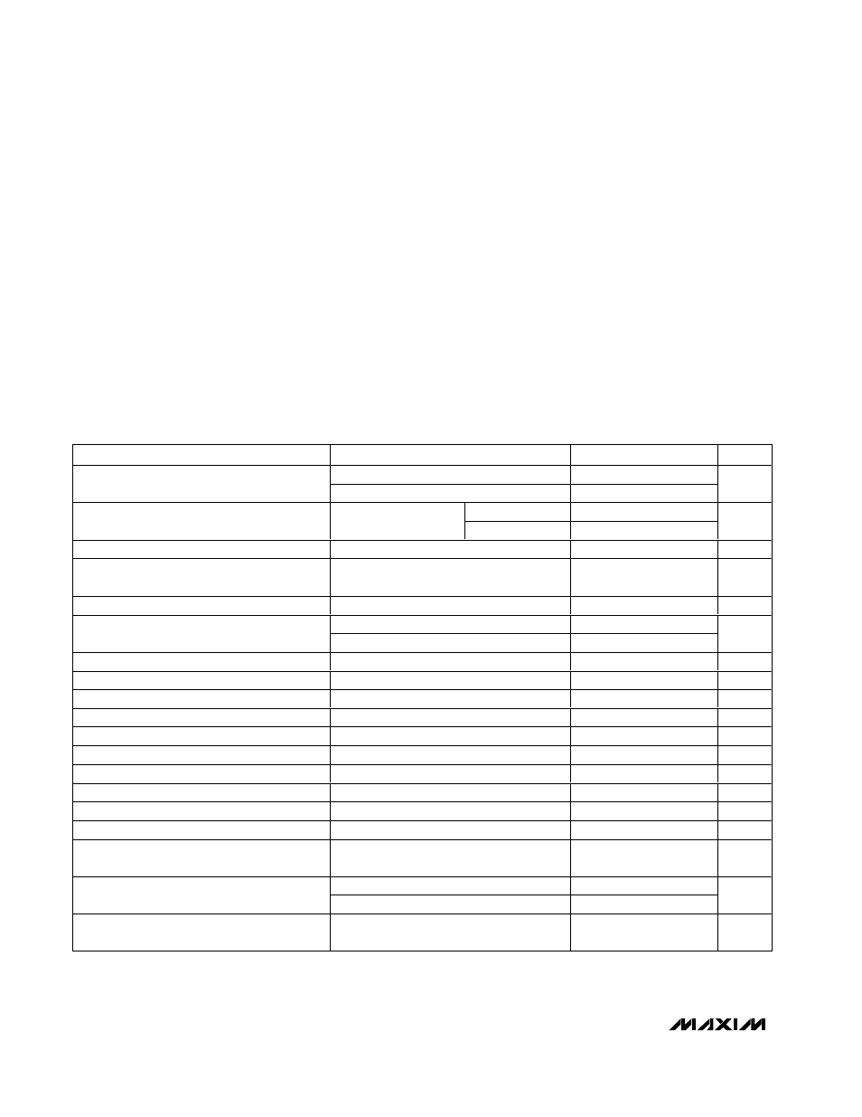
ELECTRICAL CHARACTERISTICS
(Circuit of Figure 1. V
BATT
= 12V, V
LOT
= V
REF
, V
CC
= V
DD,
V
SUS
= 5.3V,
T
A
= 0°C to +85°C. Typical values are at T
A
= +25°C,
unless otherwise noted.)
Stresses beyond those listed under “Absolute Maximum Ratings” may cause permanent damage to the device. These are stress ratings only, and functional
operation of the device at these or any other conditions beyond those indicated in the operational sections of the specifications is not implied. Exposure to
absolute maximum rating conditions for extended periods may affect device reliability.
BATT to GND..........................................................-0.3V to +30V
BST1, BST2 to GND ...............................................-0.3V to +36V
BST1 to LX1, BST2 to LX2 ........................................-0.3V to +6V
GH1 to LX1 ..............................................-0.3V to (V
BST1
+ 0.3V)
GH2 to LX2 ..............................................-0.3V to (V
BST2
+ 0.3V)
V
CC
, V
DD
to GND .....................................................-0.3V to +6V
REF, ILIM to GND .......................................-0.3V to (V
CC
+ 0.3V)
GL1, GL2 to GND .......................................-0.3V to (V
DD
+ 0.3V)
CCI, CCV, LOT to GND ............................................-0.3V to +6V
IFB, ISEC, VFB to GND................................................-6V to +6V
SDA, SCL, SUS to GND............................................-0.3V to +6V
PGND to GND .......................................................-0.3V to +0.3V
Continuous Power Dissipation (T
A
= +70°C)
28-Pin Thin QFN (derate 20.84mW/°C above +70°C) ..1667mW
Operating Temperature Range ...........................-40°C to +85°C
Junction Temperature ......................................................+150°C
Storage Temperature Range .............................-65°C to +150°C
Lead Temperature (soldering, 10s) .................................+300°C
PARAMETER
CONDITIONS
MIN
TYP
MAX
UNITS
V
CC
= V
DD
= V
BATT
4.6
5.5
V
BATT
Input Voltage Range
V
CC
= V
DD
= open
5.5
28.0
V
V
BATT
= 28V
1.5
3
V
BATT
Quiescent Current
V
SUS
= 5.5V
V
BATT
= V
CC
= 5V
3
mA
V
BATT
Quiescent Current, Shutdown
SUS = GND
6
20
µA
V
CC
Output Voltage, Normal Operation
V
SUS
= 5.5V, 6V < V
BATT
< 28V,
0 < I
LOAD
< 20mA
5.0
5.35
5.5
V
V
CC
Output Voltage, Shutdown
SUS = GND, no load
3.5
4.6
5.5
V
V
CC
rising (leaving lockout)
4.5
V
CC
Undervoltage-Lockout Threshold
V
CC
falling (entering lockout)
4.0
V
V
CC
Undervoltage-Lockout Hysteresis
200
mV
V
CC
Power-On Reset (POR) Threshold
Rising edge
0.90
1.75
2.70
V
V
CC
POR Hysteresis
50
mV
REF Output Voltage, Normal Operation
4.5V < V
CC
< 5.5V, I
LOAD
= 40µA
1.96
2.00
2.04
V
GH1, GH2, GL1, GL2 On-Resistance
I
TEST
= 100mA, V
CC
= V
DD
= 5.3V
9
18
Ω
GH1, GH2, GL1, GL2 Output Current
0.5
A
BST1, BST2 Leakage Current
V
BST
_ = 12V, V
LX
_ = 7V
5
µA
Input Resonant Frequency
Guaranteed by design
25
300
kHz
Minimum Off-Time
180
280
380
ns
Maximum Off-Time
18
28
38
µs
Current-Limit Threshold
LX1 - GND, LX2 - GND (Fixed)
ILIM = V
CC
180
200
220
mV
V
ILIM
= 0.5V
80
100
120
Current-Limit Threshold
LX1 - GND, LX2 - GND (Adjustable)
V
ILIM
= 2.0V
370
400
430
mV
Minimum Current Threshold
LX1 - GND, LX2 - GND
6
mV