Rainbow Electronics MAX5048 User Manual
Page 7

MAX5048
7.6A, 12ns, SOT23 MOSFET Driver
_______________________________________________________________________________________
7
The quiescent current is 0.95mA typical. The current
required to charge and discharge the internal nodes is
frequency dependent (see the Typical Operating
Characteristics). The MAX5048A/MAX5048B power dis-
sipation when driving a ground referenced resistive
load is:
P = D x R
ON(MAX)
x I
LOAD2
where D is the fraction of the period the MAX5048A/
MAX5048Bs’ output pulls high, R
ON (MAX)
is the maxi-
mum on-resistance of the device with the output high
(P-channel), and I
LOAD
is the output load current of the
MAX5048A/MAX5048B.
For capacitive loads, the power dissipation is:
P = C
LOAD
x (V+)
2
x FREQ
where C
LOAD
is the capacitive load, V+ is the supply
voltage, and FREQ is the switching frequency.
Layout Information
The MOSFET drivers MAX5048A/MAX5048B source-
and-sink large currents to create very fast rise and fall
edges at the gate of the switching MOSFET. The high
di/dt can cause unacceptable ringing if the trace
lengths and impedances are not well controlled. The
following PC board layout guidelines are recommended
when designing with the MAX5048A/MAX5048B:
• Place one or more 0.1µF decoupling ceramic capaci-
tor(s) from V+ to GND as close to the device as possi-
ble. At least one storage capacitor of 10µF (min)
should be located on the PC board with a low resis-
tance path to the V+ pin of the MAX5048A/MAX5048B.
• There are two AC current loops formed between the
device and the gate of the MOSFET being driven.
The MOSFET looks like a large capacitance from
gate to source when the gate is being pulled low.
The active current loop is from N_OUT of the
MAX5048A/MAX5048B to the MOSFET gate to the
MOSFET source and to GND of the MAX5048A/
MAX5048B. When the gate of the MOSFET is being
pulled high, the active current loop is from P_OUT of
the MAX5048A/MAX5048B to the MOSFET gate to
the MOSFET source to the GND terminal of the
decoupling capacitor to the V+ terminal of the
decoupling capacitor and to the V+ terminal of the
MAX5048A/MAX5048B. While the charging current
loop is important, the discharging current loop is crit-
ical. It is important to minimize the physical distance
and the impedance in these AC current paths.
IN+
V
IL
90%
10%
t
D–OFF
P_OUT AND
N_OUT
TIED
TOGETHER
t
D–ON
t
F
t
R
IN+
IN-
V+
V+
C
L
N_OUT
GND
P_OUT
TEST CIRCUIT
TIMING DIAGRAM
MAX5048A
MAX5048B
INPUT
OUTPUT
V
IH
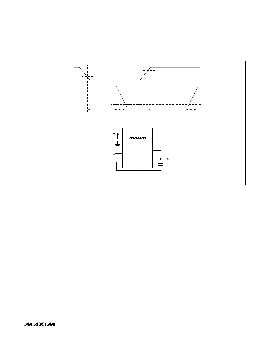
Figure 1. Timing Diagram and Test Circuit
