Detailed description, Pin description (continued) – Rainbow Electronics MAX5066 User Manual
Page 9
MAX5066
Configurable, Single-/Dual-Output, Synchronous
Buck Controller for High-Current Applications
_______________________________________________________________________________________
9
Detailed Description
The MAX5066 switching power-supply controller can
be configured in two ways. With the MODE input high, it
operates as a single-output, dual-phase, step-down
switching regulator where each output is 180° out of
phase. With the MODE pin connected low, the
MAX5066 operates as a dual-output, step-down switch-
ing regulator. The average current-mode control topolo-
gy of the MAX5066 offers high-noise immunity while
having benefits similar to those of peak current-mode
control. Average current-mode control has the intrinsic
ability to accurately limit the average current sourced
by the converter during a fault condition. When a fault
condition occurs, the error amplifier output voltage
(EAOUT1 or EAOUT2) that connects to the positive
input of the transconductance amplifier (CA1 or CA2) is
clamped thus limiting the output current.
The MAX5066 contains all blocks necessary for two
independently regulated average current-mode PWM
regulators. It has two voltage error amplifiers (VEA1
and VEA2), two current-error amplifiers (CEA1 and
CEA2), two current-sensing amplifiers (CA1 and CA2),
two PWM comparators (CPWM1 and CPWM2), and dri-
vers for both low- and high-side power MOSFETs (see
Figure 1). Each PWM section is also equipped with a
pulse-by-pulse, current-limit protection and a fault inte-
gration block for hiccup protection.
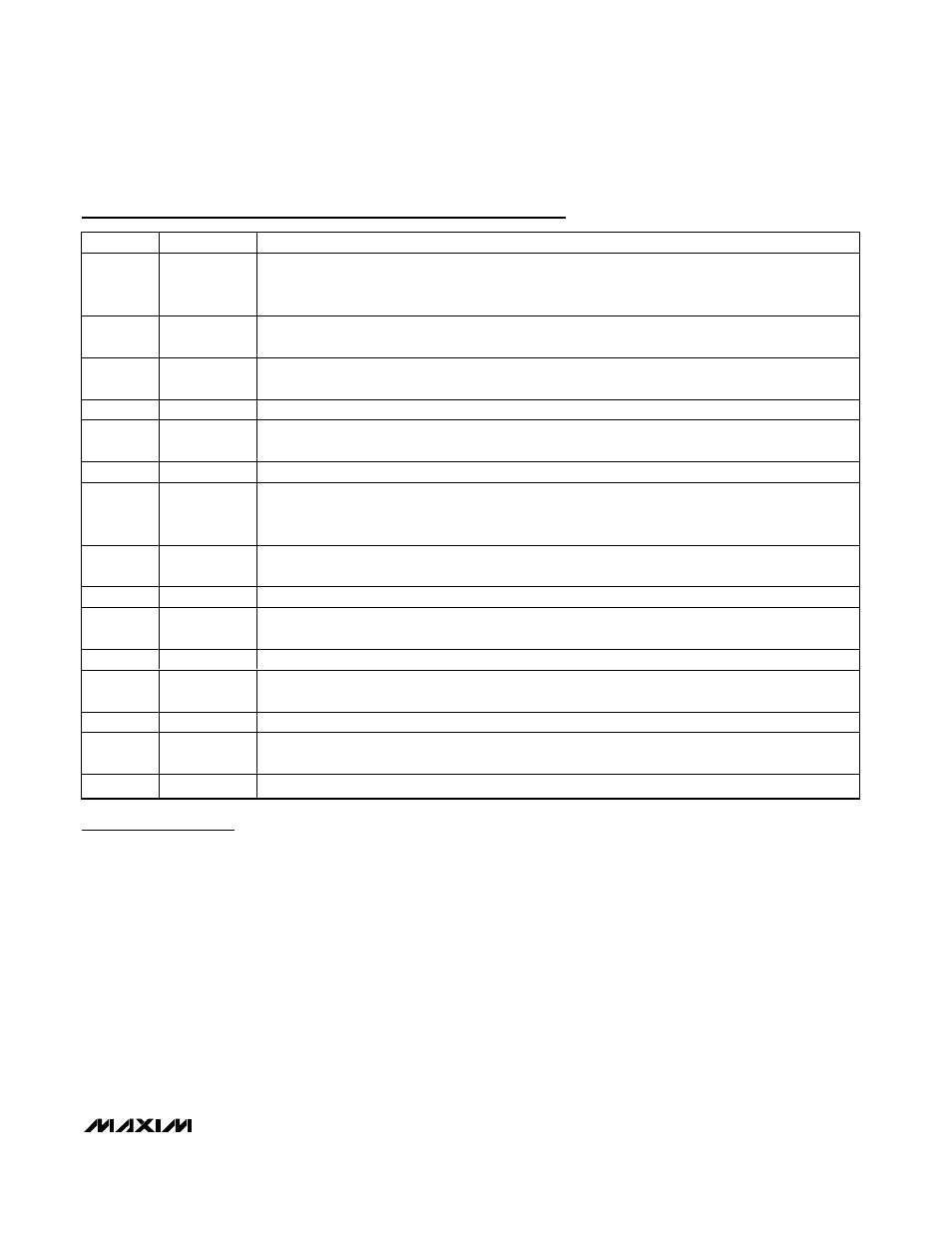
Pin Description (continued)
PIN
NAME
FUNCTION
14
CSN1
Current-Sense Differential Amplifier Negative Input for Output1. Connect CSN1 to the negative
terminal of the sense resistor. The differential voltage between CSP1 and CSN1 is internally amplified
by the current-sense amplifier (A
V(CS)
= 36V/V).
15, 28
EN
Output Enable. A logic low shuts down both channel MOSFET drivers. Pins 15 and 28 must be tied
together externally.
16
BST1
Boost Flying Capacitor Connection. Reservoir capacitor connection for the high-side MOSFET driver
supply. Connect a 0.47µF ceramic capacitor between BST1 and LX1.
17
DH1
High-Side Gate Driver Output1. DH1 drives the gate of the high-side MOSFET.
18
LX1
External inductor connection and source connection for the high-side MOSFET for Output1. LX1 also
serves as the return terminal for the high-side MOSFET driver.
19
DL1
Low-Side Gate Driver Output1. Gate driver output for the synchronous MOSFET.
20
V
DD
Supply Voltage for Low-Side Drivers. REG powers V
DD
. Connect a parallel combination of 0.1µF and
1µF ceramic capacitors from V
DD
to PGND and a 1
Ω resistor from V
DD
to REG to filter out the high-
peak currents of the driver from the internal circuitry.
21
REG
Internal 5V Regulator Output. REG is derived internally from IN and is used to power the internal bias
circuitry. Bypass REG to AGND with a 4.7µF ceramic capacitor.
22
IN
Supply Voltage Connection. Connect IN to a 5V to 28V input supply.
23
PGND
Power Ground. Source connection for the low-side MOSFET. Connect V
DD
’s bypass capacitor returns
to PGND.
24
DL2
Low-Side Gate Driver Output2. Gate driver for the synchronous MOSFET.
25
LX2
External inductor connection and source connection for the high-side MOSFET for Output2. Also
serves as the return terminal for the high-side MOSFET driver.
26
DH2
High-Side Gate Driver Output2. DH2 drives the gate of the high-side MOSFET.
27
BST2
Boost Flying Capacitor Connection. Reservoir capacitor connection for the high-side MOSFET driver
supply. Connect a 0.47µF ceramic capacitor between BST2 and LX2.
EP
EP
Exposed Pad. Connect exposed pad to ground plane.