Table 1. high-side mosfet losses – Rainbow Electronics MAX5066 User Manual
Page 18
MAX5066
Configurable, Single-/Dual-Output, Synchronous
Buck Controller for High-Current Applications
18
______________________________________________________________________________________
the highest output power needs to be used in determin-
ing the maximum input RMS ripple current requirement.
Increasing the output current drawn from the other out-
of-phase controller section results in reducing the input
ripple current. A low-ESR input capacitor that can han-
dle the maximum input RMS ripple current of one chan-
nel must be used. The maximum RMS capacitor ripple
current is given by:
where I
MAX
is the full load current of the regulator.
V
OUT
is the output voltage of the same regulator and
C
IN
is C5 in Figure 6. The ESR of the input capacitors
wastes power from the input and heats up the capaci-
tor. Reducing the ESR is important to maintain a high
overall efficiency and in reducing the heating of the
capacitors.
Output Capacitors
The worst-case peak-to-peak inductor ripple current,
the allowable peak-to-peak output ripple voltage, and
the maximum deviation of the output voltage during
step loads determine the capacitance and the ESR
requirements for the output capacitors. The output rip-
ple can be approximated as the inductor current ripple
multiplied by the output capacitor’s ESR (R
ESR_OUT
).
The peak-to-peak inductor current ripple is given by:
During a load step, the allowable deviation of the out-
put voltage during the fast transient load dictates the
output capacitance and ESR. The output capacitors
supply the load step until the controller responds with a
greater duty cycle. The response time (t
RESPONSE
)
depends on the closed-loop bandwidth of the regula-
tor. The resistive drop across the capacitor’s ESR and
capacitor discharge causes a voltage drop during a
∆I
V
D
L f
L
OUT
SW
=
−
×
(
)
1
I
I
V
V
V
V
CIN RMS
MAX
OUT
IN
OUT
IN
(
)
(
)
≈
−
LOSS
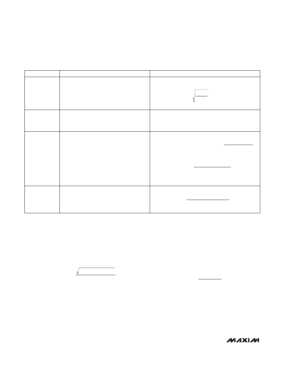
DESCRIPTION
SEGMENT LOSS
Conduction Loss
Losses associated with MOSFET on-time and
on-resistance. I
RMS
is a function of load current
and duty cycle.
Gate Drive Loss
Losses associated with charging and
discharging the gate capacitance of the
MOSFET every cycle. Use the MOSFET’s (Q
G
)
specification.
Switching Loss
Losses during the drain voltage and drain
current transitions for every switching cycle.
Losses occur only during the Q
GS2
and Q
GD
time period and not during the initial Q
GS1
period. The initial Q
GS1
period is the rise in the
gate voltage from zero to V
TH.
R
DH
is the high-side MOSFET driver’s on-
resistance and R
GATE
is the internal gate
resistance of the high-side MOSFET (Q
GD
and
Q
GS2
are found in the MOSFET data sheet).
Output Loss
Losses associated with Q
OSS
of the MOSFET
occur every cycle when the high-side MOSFET
turns on. The losses are caused by both
MOSFETs but are dissipated in the high-side
MOSFET.
Table 1. High-Side MOSFET Losses
P
I
R
where I
V
V
I
CONDUCTION
RMS
DS ON
RMS
OUT
IN
LOAD
=
Ч
≈
Ч
2
(
)
P
V
Q
f
GATEDRIVE
DD
G
SW
=
Ч
Ч
P
V
I
f
Q
Q
I
SWITCH
IN
LOAD
SW
GS
GD
GATE
=
Ч
Ч
Ч
+
2
(
)
where I
V
R
R
GATE
DD
DH
GATE
=
×
+
2 (
)
P
Q
Q
V
f
OUTPUT
OSS HS
OSS LS
IN
SW
=
+
Ч
Ч
2
(
)
(
)