Table 2. low-side mosfet losses – Rainbow Electronics MAX5066 User Manual
Page 19
MAX5066
Configurable, Single-/Dual-Output, Synchronous
Buck Controller for High-Current Applications
______________________________________________________________________________________
19
load step. Use a combination of SP polymer and
ceramic capacitors for better transient load and rip-
ple/noise performance.
Keep the maximum output-voltage deviation less than
or equal to the adaptive voltage-positioning window
(
∆V
OUT
). During a load step, assume a 50% contribu-
tion each from the output capacitance discharge and
the voltage drop across the ESR (
∆V
OUT
=
∆V
ESR_OUT
+
∆V
Q_OUT
). Use the following equations to calculate
the required ESR and capacitance value:
where I
LOAD_STEP
is the step in load current and
t
RESPONSE
is the response time of the controller.
Controller response time depends on the control-loop
bandwidth. C
OUT
is C6 and C7 in Figure 6.
Current Limit
The average current-mode control technique of the
MAX5066 accurately limits the maximum average out-
put current per phase. The MAX5066 senses the volt-
age across the sense resistor and limits the maximum
inductor current accordingly. Use the equations below
to calculate the current-sense resistor values:
Due to tolerances involved, the minimum average volt-
age at which the voltage across the current-sense
resistor is clamped is 20.4mV. Therefore, the minimum
average current limit is set at:
For example, the current-sense resistor:
for a maximum output current of 10A. The standard
value is 2m
Ω. Also, adjust the value of the current-
sense resistor to compensate for parasitics associated
with the PC board. Select a noninductive resistor with
appropriate wattage rating.
The second type of current limit is the peak current limit
as explained in the Peak-Current Comparator section.
The third current-protection circuit is the hiccup fault
protection as explained in the Hiccup Fault Protection
section. The average current during a short at the out-
put is given by:
Reverse Current Limit
The MAX5066 limits the reverse current when the output
capacitor voltage is higher than the preset output volt-
age. Calculate the maximum reverse current limit based
on V
CLAMP_LO
and the current-sense resistor R
SENSE
.
I
R
AVG SHORT
SENSE
(
)
.
=
×
−
1 41
10
3
R
mV
A
m
SENSE
=
=
20 4
10
2 04
.
.
Ω
I
R
LIMIT MIN
SENSE
(
)
.
=
×
−
20 4
10
3
I
R
LOAD MAX
SENSE
(
)
.
=
×
−
24 75
10
3
R
V
I
C
I
t
V
ESR OUT
ESR OUT
LOAD STEP
OUT
LOAD STEP
RESPONSE
Q OUT
_
_
_
_
_
=
=
×
∆
∆
LOSS
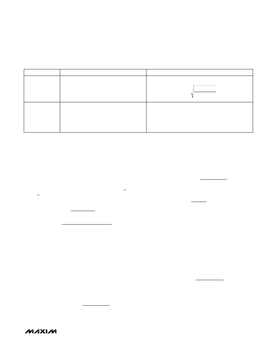
DESCRIPTION
SEGMENT LOSSES
Conduction Loss
Losses associated with MOSFET on-time, I
RMS
is a function of load current and duty cycle.
Gate Drive Loss
Losses associated with charging and
discharging the gate of the MOSFET every
cycle. There is no Q
GD
charging involved in this
MOSFET due to the zero-voltage turn-on. The
charge involved is (Q
G
- Q
GD
).
Table 2. Low-Side MOSFET Losses
P
I
R
where I
V
V
V
I
CONDUCTION
RMS
DS ON
RMS
IN
OUT
IN
LOAD
=
Ч
≈
−
Ч
2
(
)
P
V
Q
Q
f
GATEDRIVE
DD
G
GD
SW
=
Ч
−
Ч
(
)
Note: The gate drive losses are distributed between the drivers and the MOSFETs in the ratio of the gate driver’s resistance and the
MOSFET’s internal gate resistance.