Control loop – Rainbow Electronics MAX5066 User Manual
Page 12
MAX5066
Configurable, Single-/Dual-Output, Synchronous
Buck Controller for High-Current Applications
12
______________________________________________________________________________________
blocks that enable “hiccuping” under overcurrent con-
ditions. This circuit works as follows: for every clock
cycle the current-limit threshold is exceeded, the fault
integration counter increments by one count. Thus, if
the current-limit condition persists, then the counter
reaches its shutdown threshold in 32,768 counts and
shuts down the external MOSFETs. When the MAX5066
shuts down due to a fault, the counter begins to count
down, (since the current-limit condition has ended),
once every 16 clock cycles. Thus, the device counts
down for 524,288 clock cycles. At this point, switching
resumes. This produces an effective duty cycle of
6.25% power-up and 93.75% power-down under fault
conditions. With a switching frequency set to 250kHz,
power-up and power-down times are approximately
131ms and 2.09s, respectively.
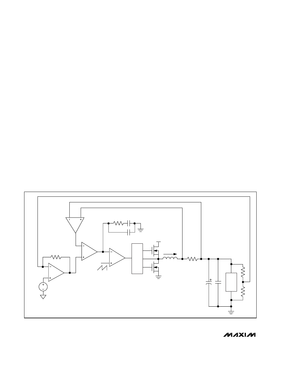
Control Loop
The MAX5066 uses an average current-mode control
topology to regulate the output voltage. The control
loop consists of an inner current loop and an outer volt-
age loop. The inner current loop controls the output
current, while the outer voltage loop controls the output
voltage. The inner current loop absorbs the inductor
pole, reducing the order of the outer voltage loop to
that of a single-pole system. Figure 2 is the block dia-
gram of OUT1’s control loop.
The current loop consists of a current-sense resistor,
R
SENSE
, a current-sense amplifier (CA1), a current-
error amplifier (CEA1), an oscillator providing the carri-
er ramp, and a PWM comparator (CPWM1). The
precision current-sense amplifier (CA1) amplifies the
sense voltage across R
SENSE
by a factor of 36. The
inverting input to CEA1 senses the output of CA1. The
output of CEA1 is the difference between the voltage-
error amplifier output (EAOUT1) and the gained-up volt-
age from CA1. The RC compensation network
connected to CLP1 provides external frequency com-
pensation for the respective CEA1 (see the
Compensation section). The start of every clock cycle
enables the high-side driver and initiates a PWM on-
cycle. Comparator CPWM1 compares the output volt-
age from CEA1 against a 0 to 2V ramp from the
oscillator. The PWM on-cycle terminates when the ramp
voltage exceeds the error voltage from the current-error
amplifier (CEA1).
DRIVE
V
IN
V
OUT1
C
OUT
V
REF
= 0.61V
R
F
C
CFF
C
CF
I
L
R
CF
CSN1
CSP1
CLP1
2V
P-P
R
SENSE
LOAD
R1
R2
CA 1
CEA1
CPWM1
VEA1
Figure 2. Current and Voltage Loops