And v – Rainbow Electronics MAX5066 User Manual
Page 10
MAX5066
Configurable, Single-/Dual-Output, Synchronous
Buck Controller for High-Current Applications
10
______________________________________________________________________________________
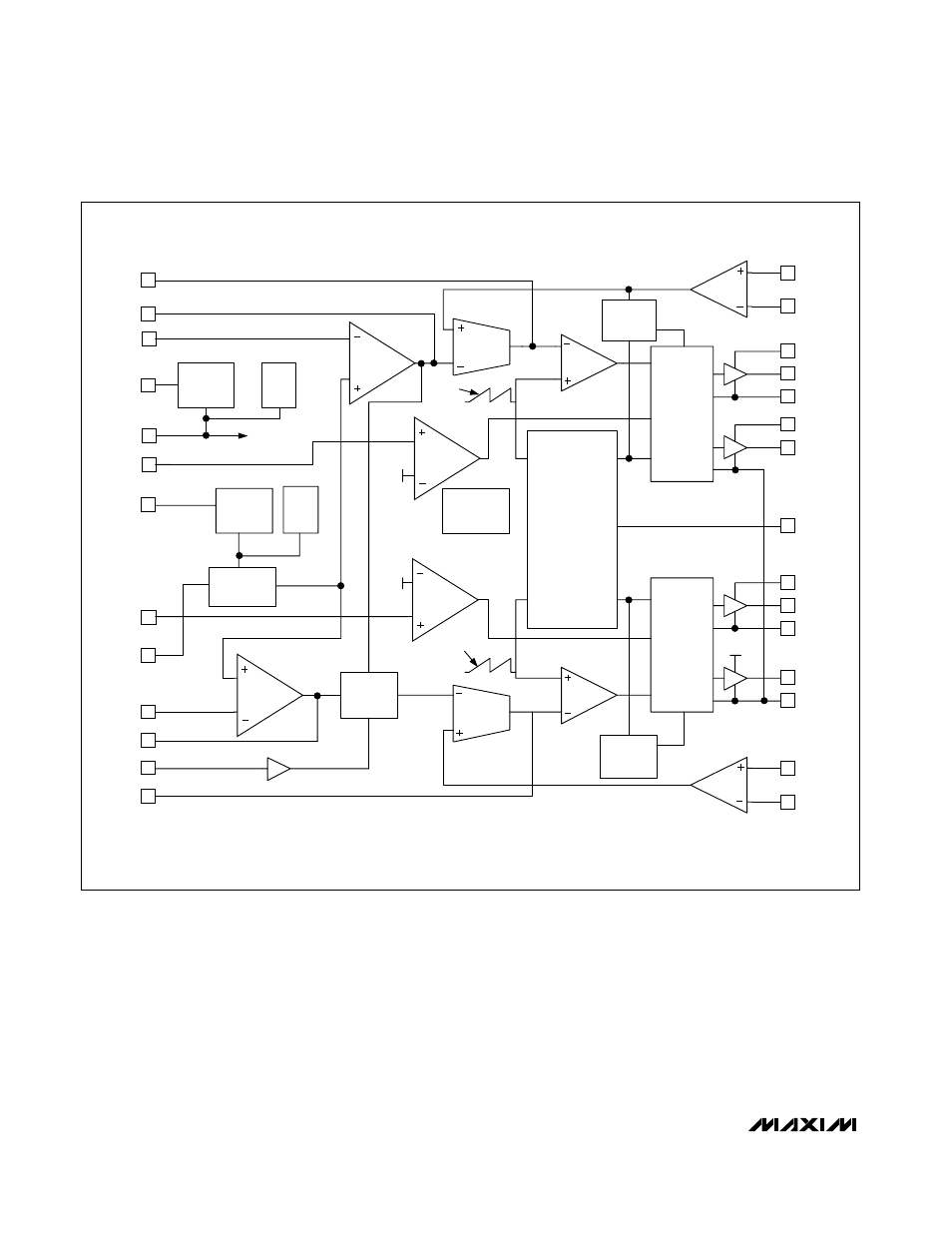
An oscillator, with an externally programmable frequen-
cy generates two clock pulse trains and two ramps for
both PWM sections. The two clocks and the two ramps
are 180° out of phase with each other.
A linear regulator (REG) generates the 5V to supply the
device. This regulator has the output-current capability
necessary to provide for the MAX5066’s internal circuit-
ry and the power for the external MOSFET’s gate dri-
vers. A low-current linear regulator (REF) provides a
precise 3.3V reference output and is capable of driving
loads of up to 200µA. Internal UVLO circuitry ensures
that the MAX5066 starts up only when V
REG
and V
REF
are at the correct voltage levels to guarantee safe oper-
ation of the IC and of the power MOSFETs.
Finally, a thermal-shutdown feature protects the device
during thermal faults and shuts down the MAX5066
when the die temperature exceeds +160°C.
16
17
18
19
BST1
DH1
LX1
DL1
20
27
26
25
24
23
BST2
DH2
LX2
DL2
PGND
V
DD
2 CSP2
1 CSN2
13 CSP1
14 CSN1
CA1
11
EAN1
6
REF
AGND
8
EN
15
EN
28
CA2
CPWM1
CPWM2
7 RT/CLKIN
CEA1
CEA2
12
EAOUT1
9
MODE
3
EAOUT2
5
CLP2
10
CLP1
22
IN
21
REG
1.225V
1.225V
THERMAL
SHUTDOWN
V
DD
MUX
4
EAN2
CEN
VEA1
DF1 AND
HICCUP
LOGIC
EXTERNAL FREQUENCY SYNC
0
°
CONTROL
AND DRIVER
LOGIC 1
CONTROL
AND DRIVER
LOGIC 2
DF2 AND
HICCUP
LOGIC
OSCILLATOR
AND PHASE
SPLITTER
180
°
2V
P-P
RAMP
V
REG
= 5V
FOR INTERNAL
BIASING
UVLO
V
REF
= 3.3V
UV33
V
INTREF
= 0.61V
VEA2
CEN
2V
P-P
RAMP
Figure 1. Block Diagram