Ac electrical characteristics – Rainbow Electronics ADC12062 User Manual
Page 4
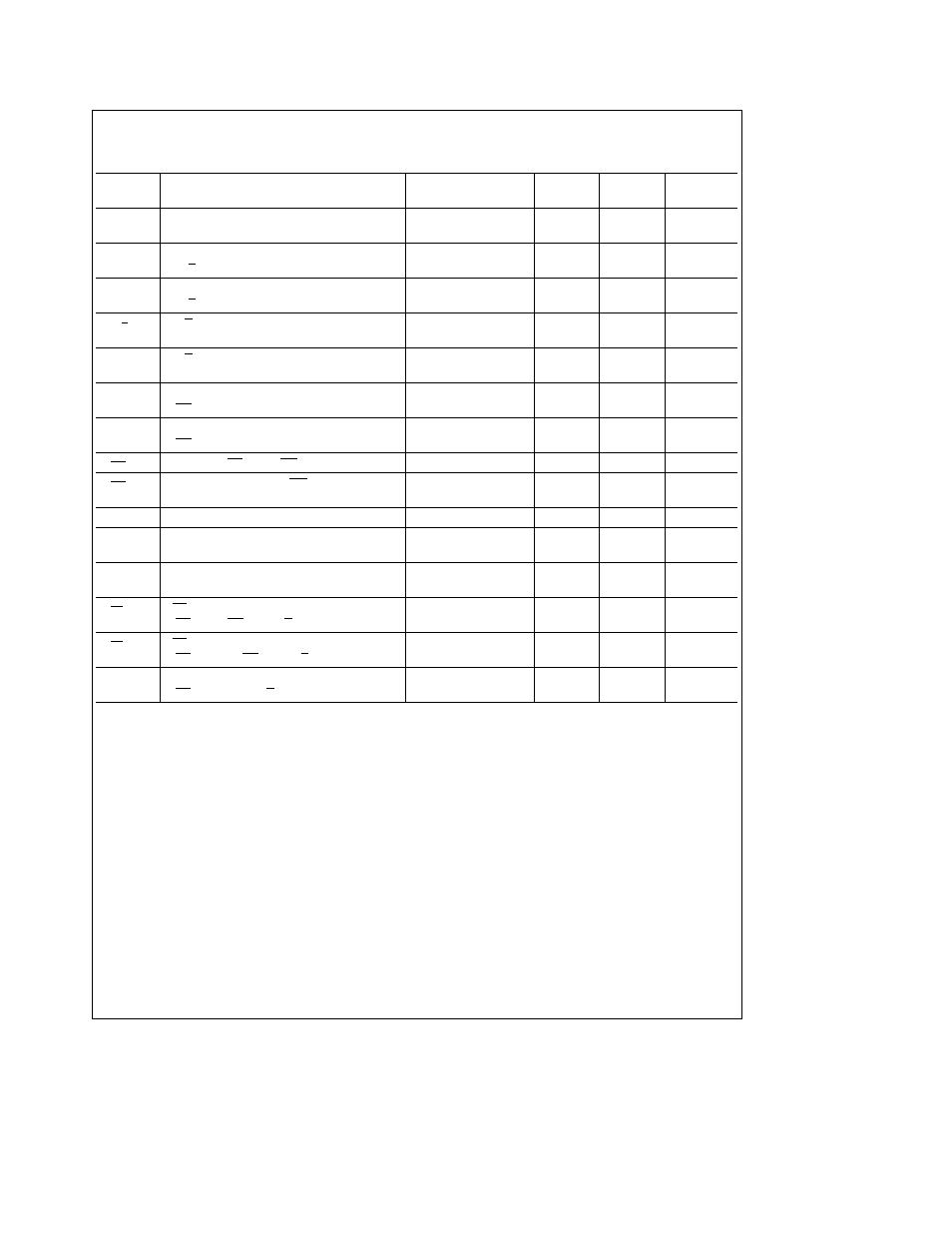
AC Electrical Characteristics
The following specifications apply for DV
CC
e
AV
CC
e
a
5V
V
REF
a
(SENSE)
e a
4 096V V
REF
b
(SENSE)
e
AGND and f
s
e
1 MHz unless otherwise specified Boldface limits apply
for T
A
e
T
J
from T
MIN
to T
MAX
all other limits T
A
e
T
J
e a
25 C
Symbol
Parameter
Conditions
Typ
Limit
Units
(Note 7)
(Note 8)
(Limits)
f
s
Maximum Sampling Rate
1
MHz (min)
(1 t
THROUGHPUT
)
t
CONV
Conversion Time
740
600
ns (min)
(S H Low to EOC High)
980
ns (max)
t
AD
Aperture Delay
20
ns
(S H Low to Input Voltage Held)
t
S H
S H Pulse Width
5
ns (min)
550
ns (max)
t
EOC
S H Low to EOC Low
95
60
ns (min)
125
ns (max)
t
ACC
Access Time
C
L
e
100 pF
10
20
ns (max)
(RD Low or OE High to Data Valid)
t
1H
t
0H
TRI-STATE Control
R
L
e
1k C
L
e
10 pF
25
40
ns (max)
(RD High or OE Low to Databus TRI-STATE)
t
INTH
Delay from RD Low to INT High
C
L
e
100 pF
35
60
ns (max)
t
INTL
Delay from EOC High to INT Low
C
L
e
100 pF
b
25
b
35
ns (min)
b
10
ns (max)
t
UPDATE
EOC High to New Data Valid
5
15
ns (max)
t
MS
Multiplexer Address Setup Time
50
ns (min)
(MUX Address Valid to EOC Low)
t
MH
Multiplexer Address Hold Time
50
ns (min)
(EOC Low to MUX Address Invalid)
t
CSS
CS Setup Time
20
ns (min)
(CS Low to RD Low S H Low or OE High)
t
CSH
CS Hold Time
20
ns (min)
(CS High after RD High S H High or OE Low)
t
WU
Wake-Up Time
1
m
s
(PD High to First S H Low)
Note 1
Absolute Maximum Ratings indicate limits beyond which damage to the device may occur Operating Ratings indicate conditions for which the device is
functional These ratings do not guarantee specific performance limits however For guaranteed specifications and test conditions see the Electrical Characteris-
tics The guaranteed specifications apply only for the test conditions listed Some performance characteristics may degrade when the device is not operated under
the listed test conditions
Note 2
All voltages are measured with respect to GND (GND
e
AGND
e
DGND) unless otherwise specified
Note 3
When the input voltage (V
IN
) at any pin exceeds the power supply rails (V
IN
k
GND or V
IN
l
V
CC
) the absolute value of current at that pin should be
limited to 25 mA or less The 50 mA package input current limits the number of pins that can safely exceed the power supplies with an input current of 25 mA to
two
Note 4
The maximum power dissipation must be derated at elevated temperatures and is dictated by T
JMAX
i
JA
and the ambient temperature T
A
The maximum
allowable power dissipation at any temperature is P
D
e
(T
JMAX
b
T
A
) i
JA
or the number given in the Absolute Maximum Ratings whichever is lower i
JA
for the V
(PLCC) package is 55 C W i
JA
for the VF (PQFP) package is 62 C W In most cases the maximum derated power dissipation will be reached only during fault
conditions
4