Applications information – Rainbow Electronics ADC12062 User Manual
Page 13
Applications Information
(Continued)
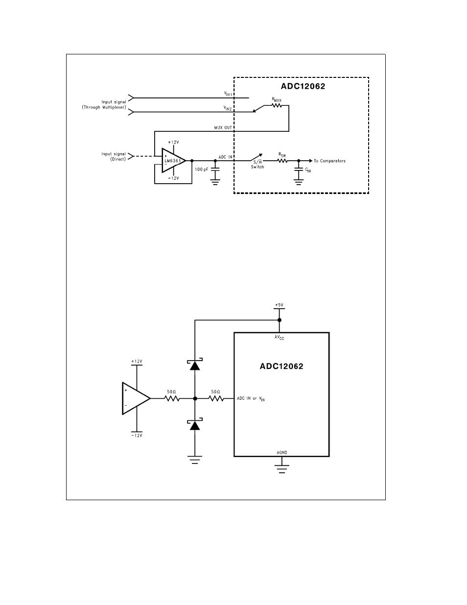
TL H 11490 – 18
FIGURE 8 Buffering the Input with an LM6361 High Speed Op Amp
Another benefit of using a high speed buffer is improved
THD performance when using the multiplexer of the
ADC12062 The MUX on-resistance is somewhat non-linear
over input voltage causing the RC time constant formed by
C
IN
R
MUX
and R
SW
to vary depending on the input voltage
This results in increasing THD with increasing frequency
Inserting the buffer between the MUX OUT and the ADC IN
terminals as shown in
Figure 8
will eliminate the loading on
R
MUX
significantly reducing the THD of the multiplexed sys-
tem
Correct converter operation will be obtained for input volt-
ages greater than AGND b 50 mV and less than AV
CC
a
50 mV Avoid driving the signal source more than 300 mV
higher than AV
CC
or more than 300 mV below AGND If an
analog input pin is forced beyond these voltages the cur-
rent flowing through that pin should be limited to 25 mA or
less to avoid permanent damage to the IC The sum of all
the overdrive currents into all pins must be less than 50 mA
When the input signal is expected to extend more than
300 mV beyond the power supply limits for any reason (un-
known uncontrollable input voltage range power-on tran-
sients fault conditions etc ) some form of input protection
such as that shown in
Figure 9
should be used
TL H 11490 – 19
FIGURE 9 Input Protection
13