Applications information – Rainbow Electronics ADC12062 User Manual
Page 16
Applications Information
(Continued)
5 0 POWER SUPPLY CONSIDERATIONS
The ADC12062 is designed to operate from a single a5V
power supply There are two analog supply pins (AV
CC
) and
one digital supply pin (DV
CC
) These pins allow separate
external bypass capacitors for the analog and digital por-
tions of the circuit To guarantee proper operation of the
converter all three supply pins should be connected to the
same voltage source In systems with separate analog and
digital supplies the converter should be powered from the
analog supply
The ground pins are AGND (analog ground) DGND1 (digital
input ground) and DGND2 (digital output ground) These
pins allow for three separate ground planes for these sec-
tions of the chip Isolating the analog section from the two
digital sections reduces digital interference in the analog cir-
cuitry improving the dynamic performance of the converter
Separating the digital outputs from the digital inputs (particu-
larly the S H input) reduces the possibility of ground bounce
from the 12 data lines causing jitter on the S H input The
analog ground plane should be connected to the Digital2
ground plane at the ground return for the power supply The
Digital1 ground plane should be tied to the Digital2 ground
plane at the DGND1 and DGND2 pins
Both AV
CC
pins should be bypassed to the AGND ground
plane with 0 1 mF ceramic capacitors One of the two AV
CC
pins should also be bypassed with a 10 mF tantalum capaci-
tor DV
CC
should be bypassed to the DGND2 ground pIane
with a 0 1 mF capacitor in parallel with a 10 mF tantalum
capacitor
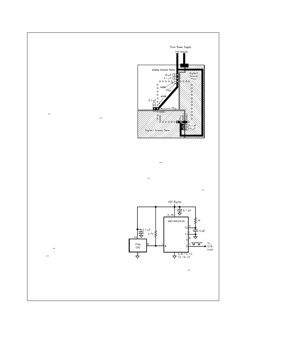
6 0 LAYOUT AND GROUNDING
In order to ensure fast accurate conversions from the
ADC12062 it is necessary to use appropriate circuit board
layout techniques
Separate analog and digital ground
planes are required to meet datasheet AC and DC limits
The analog ground plane should be low-impedance and free
of noise from other parts of the system
All bypass capacitors should be located as close to the con-
verter as possible and should connect to the converter and
to ground with short traces The analog input should be iso-
lated from noisy signal traces to avoid having spurious sig-
nals couple to the input Any external component (e g
a
filter capacitor) connected across the converter’s input
should be connected to a very clean analog ground return
point Grounding the component at the wrong point will re-
sult in increased noise and reduced conversion accuracy
Figure 12
gives an example of a suitable layout including
power supply routing ground plane separation and bypass
capacitor placement All analog circuitry (input amplifiers
filters reference components etc ) should be placed on the
analog ground plane All digital circuitry and I O lines (ex-
cluding the S H input) should use the digital2 ground plane
as ground The digital1 ground plane should only be used
for the S H signal generation
TL H 11490 – 22
FIGURE 12 PC Board Layout
7 0 DYNAMIC PERFORMANCE
The ADC12062 is AC tested and its dynamic performance is
guaranteed In order to meet these specifications the clock
source driving the S H input must be free of jitter For the
best AC performance a crystal oscillator is recommended
For operation at or near the ADC12062’s 1 MHz maximum
sampling rate a 1 MHz squarewave will provide a good sig-
nal for the S H input As long as the duty cycle is near 50%
the waveform will be low for about 500 ns which is within
the 550 ns limit When operating the ADC12062 at a sample
rate of 910 kHz or below the pulse width of the S H signal
must be smaller than half the sample period
TL H 11490 – 23
FIGURE 13 Crystal Clock Source
Figure 13
is an example of a low jitter S H pulse generator
that can be used with the ADC12062 and allow operation at
sampling rates from DC to 1 MHz A standard 4-pin DIP
crystal oscillator provides a stable 1 MHz squarewave
Since most DIP oscillators have TTL outputs a 4 7k pullup
resistor is used to raise the output high voltage to CMOS
input levels The output is fed to the trigger input (falling
16