Applications information – Rainbow Electronics ADC12062 User Manual
Page 12

Applications Information
(Continued)
TL H 11490 – 16
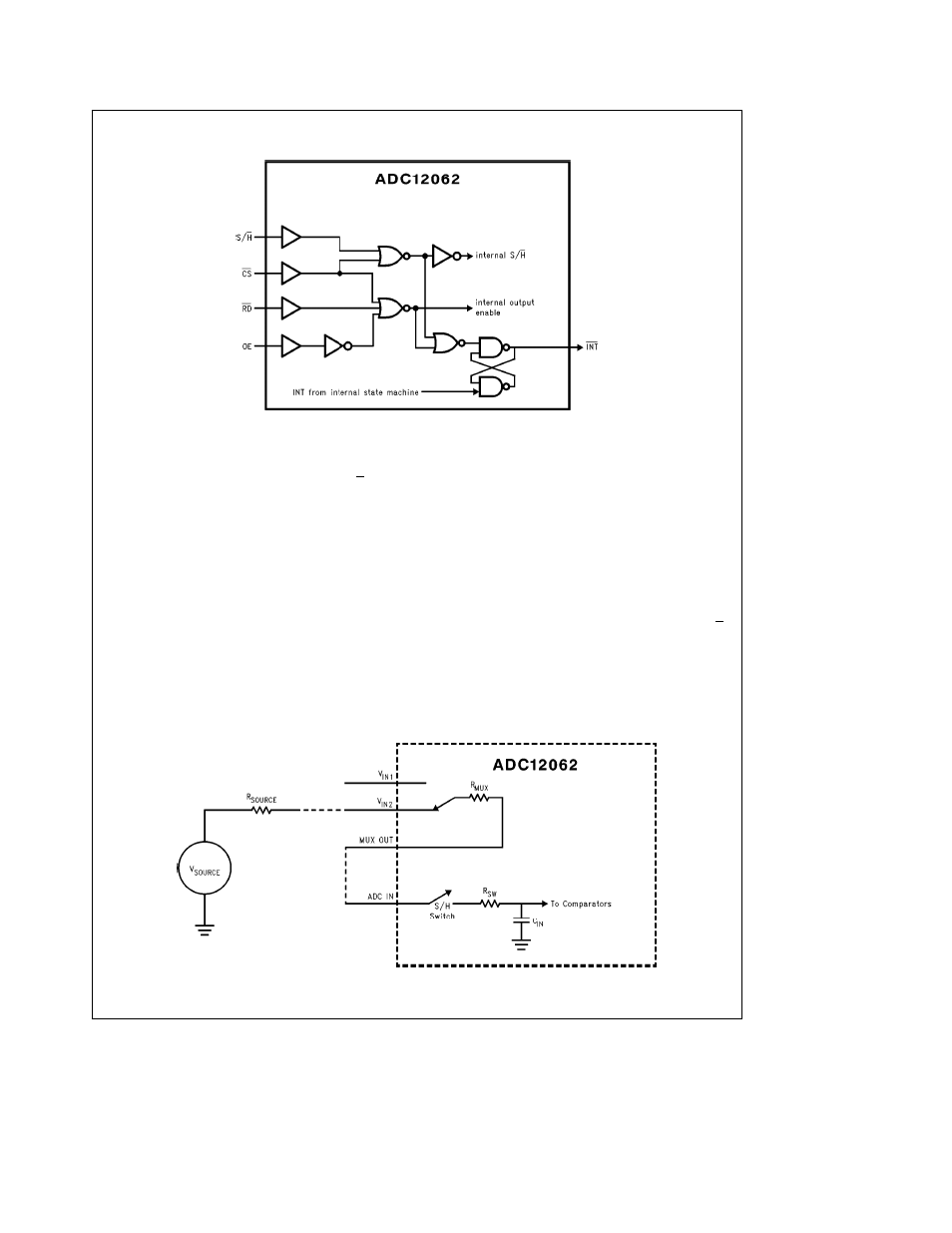
FIGURE 6 ADC Control Logic
2 0 THE ANALOG INPUT
The analog input of the ADC12062 can be modeled as two
small resistances in series with the capacitance of the input
hold capacitor (C
IN
) as shown in
Figure 7
The S H switch
is closed during the Sample period and open during Hold
The source has to charge C
IN
to the input voltage within the
sample period Note that the source impedance of the input
voltage (R
SOURCE
) has a direct effect on the time it takes to
charge C
IN
If R
SOURCE
is too large the voltage across C
IN
will not settle to within 0 5 LSBs of V
SOURCE
before the
conversion begins and the conversion results will be incor-
rect From a dynamic performance viewpoint the combina-
tion of R
SOURCE
R
MUX
R
SW
and C
IN
form a low pass
filter Minimizing R
SOURCE
will increase the frequency re-
sponse of the input stage of the converter
Typical values for the components shown in
Figure 7
are
R
MUX
e
100X R
SW
e
100X and C
IN
e
25 pF The set-
tling time to n bits is
t
SETTLE
e
(R
SOURCE
a
R
MUX
a
R
SW
)
C
IN
n
ln (2)
The bandwidth of the input circuit is
f
b
3dB
e
1 (2
3 14
(R
SOURCE
a
R
MUX
a
R
SW
)
C
IN
)
For maximum performance the impedance of the source
driving the ADC12062 should be made as small as possible
A source impedance of 100X or less is recommended A
plot of dynamic performance vs source impedance is given
in the Typical Performance Characteristics section
If the signal source has a high output impedance its output
should be buffered with an operational amplifier capable of
driving a switched 25 pF 100X load Any ringing or instabili-
ties at the op amp’s output during the sampling period can
result in conversion errors The LM6361 high speed op amp
is a good choice for this application due to its speed and its
ability to drive large capacitive loads
Figure 8
shows the
LM6361 driving the ADC IN input of an ADC12062 The
100 pF capacitor at the input of the converter absorbs some
of the high frequency transients generated by the S H
switching reducing the op amp transient response require-
ments The 100 pF capacitor should only be used with high
speed op amps that are unconditionally stable driving ca-
pacitive loads
TL H 11490 – 17
FIGURE 7 Simplified ADC12062 Input Stage
12
