Functional description, Applications information – Rainbow Electronics ADC12062 User Manual
Page 11
Functional Description
(Continued)
tap points between (
)V
REF
and (
)V
REF
This overlap of
(
)V
REF
will automatically cancel a Voltage Estimator er-
ror of up to 256 LSBs If the first flash conversion deter-
mines that the input voltage is between (
)V
REF
and
((
)V
REF
b
LSB 2) the Voltage Estimator’s output code
will be corrected by subtracting ‘‘1’’ resulting in a corrected
value of ‘‘01’’ for the first two MSBs If the first flash conver-
sion determines that the input voltage is between (
)V
REF
b
LSB 2) and (
)V
REF
the voltage estimator’s output
code is unchanged
The results of the first flash and the Voltage Estimator’s
output are given to the factory-programmed on-chip
EEPROM which returns a correction code corresponding to
the error of the MSB ladder at that tap This code is convert-
ed to a voltage by the Correction DAC To generate the next
four bits SW1 is moved to position 2 so the ladder voltage
and the correction voltage are subtracted from the input
voltage The remainder is applied to the sixteen flash con-
verters and compared with the 16 tap points from the LSB
ladder
The result of this second conversion is accurate to 10 bits
and describes the input remainder as a voltage between two
tap points (V
H
and V
L
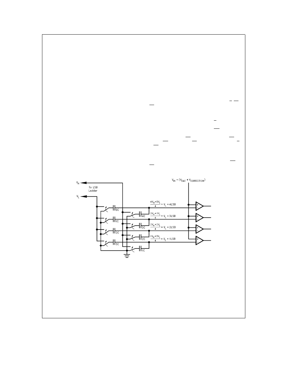
) on the LSB ladder To resolve the
last two bits the voltage across the ladder resistor (between
V
H
and V
L
) is divided up into 4 equal parts by the capacitive
voltage divider shown in
Figure 5
The divider also creates
6 LSBs below V
L
and 6 LSBs above V
H
to provide overlap
used by the digital error correction SW1 is moved to posi-
tion 3 and the remainder is compared with these 16 new
voltages The output is combined with the results of the
Voltage Estimator first flash and second flash to yield the
final 12-bit result
By using the same sixteen comparators for all three flash
conversions the number of comparators needed by the
multi-step converter is significantly reduced when compared
to standard multi-step techniques
Applications Information
1 0 MODES OF OPERATION
The ADC12062 has two interface modes An interrupt read
mode and a high speed mode
Figures 1
and
2
show the
timing diagrams for these interfaces
In order to clearly show the relationship between S H CS
RD and OE the control logic decoding section of the
ADC12062 is shown in
Figure 6
Interrupt Interface
As shown in
Figure 1
the falling edge of S H holds the input
voltage and initiates a conversion At the end of the conver-
sion the EOC output goes high and the INT output goes
low indicating that the conversion results are latched and
may be read by pulling RD low The falling edge of RD re-
sets the INT line Note that CS must be low to enable S H
or RD
High Speed Interface
This is the fastest interface shown in
Figure 2
Here the
output data is always present on the databus and the INT to
RD delay is eliminated
TL H 11490 – 15
FIGURE 5 The Capacitive Voltage Divider
11