Functional description – Rainbow Electronics ADC12062 User Manual
Page 10

Functional Description
The ADC12062 performs a 12-bit analog-to-digital conver-
sion using a 3 step flash technique The first flash deter-
mines the six most significant bits the second flash gener-
ates four more bits and the final flash resolves the two least
significant bits
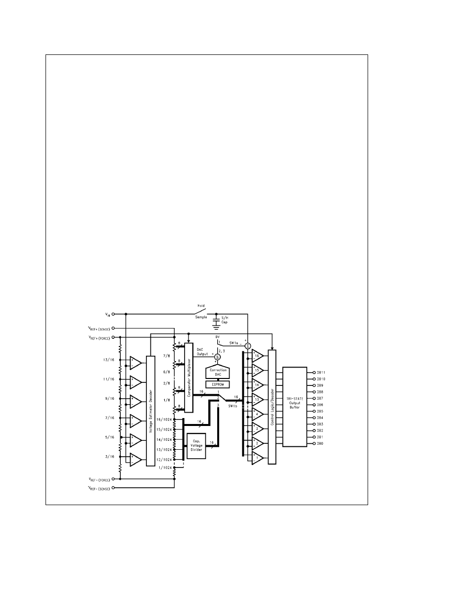
Figure 4
shows the major functional blocks
of the converter It consists of a 2
-bit Voltage Estimator a
resistor ladder with two different resolution voltage spans a
sample hold capacitor a 4-bit flash converter with front end
multiplexer a digitally corrected DAC and a capacitive volt-
age divider
The resistor string near the center of the block diagram in
Figure 4
generates the 6-bit and 10-bit reference voltages
for the first two conversions Each of the 16 resistors at the
bottom of the string is equal to
of the total string resist-
ance These resistors form the LSB Ladder and have a
voltage drop of
of the total reference voltage (V
REF
a
b
V
REF
b
) across each of them The remaining resistors
form the MSB Ladder It is comprised of eight groups of
eight resistors each connected in series (the lowest MSB
ladder resistor is actually the entire LSB ladder) Each MSB
Ladder section has
of the total reference voltage across
it Within a given MSB ladder section each of the eight MSB
resistors has
of the total reference voltage across it Tap
points are found between all of the resistors in both the
MSB and LSB ladders The Comparator MultipIexer can
connect any of these tap points in two adjacent groups of
eight to the sixteen comparators shown at the right of
Figure 4
This function provides the necessary reference
voltages to the comparators during the first two flash con-
versions
The six comparators seven-resistor string (Estimator DAC
ladder) and Estimator Decoder at the left of
Figure 4
form
Note The weight of each resistor on the LSB ladder is actually equivalent
to four 12-bit LSBs It is called the LSB ladder because it has the
highest resolution of all the ladders in the converter
the Voltage Estimator The Estimator DAC connected be-
tween V
REF
a
and V
REF
b
generates the reference volt-
ages for the six Voltage Estimator comparators The com-
parators perform a very low resoIution A D conversion to
obtain an ‘‘estimate’’ of the input voltage This estimate is
used to control the placement of the Comparator Multiplex-
er connecting the appropriate MSB ladder section to the
sixteen flash comparators A total of only 22 comparators (6
in the Voltage Estimator and 16 in the flash converter) is
required to quantize the input to 6 bits instead of the 64 that
would be required using a traditional 6-bit flash
Prior to a conversion the Sample Hold switch is closed
allowing the voltage on the S H capacitor to track the input
voItage Switch 1 is in position 1 A conversion begins by
opening the Sample Hold switch and latching the output of
the Voltage Estimator The estimator decoder then selects
two adjacent banks of tap points aIong the MSB ladder
These sixteen tap points are then connected to the sixteen
flash converters For exampIe if the input voltage is be-
tween
and
of V
REF
(V
REF
e
V
REF
a
b
V
REF
b
) the
estimator decoder instructs the comparator multiplexer to
select the sixteen tap points between
and
(
and
) of V
REF
and connects them to the sixteen comparators
The first flash conversion is now performed producing the
first 6 MSBs of data
At this point Voltage Estimator errors as large as
of
V
REF
will be corrected since the comparators are connect-
ed to ladder voltages that extend beyond the range speci-
fied by the Voltage Estimator For example if (
)V
REF
k
V
IN
k
(
)V
REF
the Voltage Estimator’s comparators
tied to the tap points below (
)V
REF
will output ‘‘1’’s
(000111) This is decoded by the estimator decoder to ‘‘10’’
The 16 comparators will be placed on the MSB ladder
TL H 11490 – 14
FIGURE 4 Functional Block Diagram
10
