Applications information – Rainbow Electronics ADC12062 User Manual
Page 14

Applications Information
(Continued)
3 0 ANALOG MULTIPLEXER
The ADC12062 has an input multiplexer that is controlled by
the logic level on pin S0 when EOC goes low as shown in
Figures 1
and
2
Multiplexer setup and hold times with re-
spect to the S H input can be determined by these two
equations
t
MS (wrt S H)
e
t
MS
b
t
EOC (min)
e
50 b 60 e b10 ns
t
MH (wrt S H)
e
t
MH
a
t
EOC (max)
e
50 a 125 e 175 ns
Note that t
MS (wrt S H)
is a negative number this indicates
that the data on S0 must become valid within 10 ns after
S H goes low in order to meet the setup time requirements
S0 must be valid for a length of
(t
MH
a
t
EOC (max)
) b (t
MS
b
t
EOC (min)
) e 185 ns
Table I shows how the input channels are assigned
TABLE I ADC12062 Input
Multiplexer Programming
S0
Channel
0
V
IN1
1
V
IN2
The output of the multiplexer is available to the user via the
MUX OUT pin This output allows the user to perform addi-
tional signal processing such as filtering or gain before the
signal is returned to the ADC IN input and digitized If no
additional signal processing is required the MUX OUT pin
should be tied directly to the ADC IN pin
See Section 9 0 (APPLICATIONS) for a simple circuit that
will alternate between the two inputs while converting at full
speed
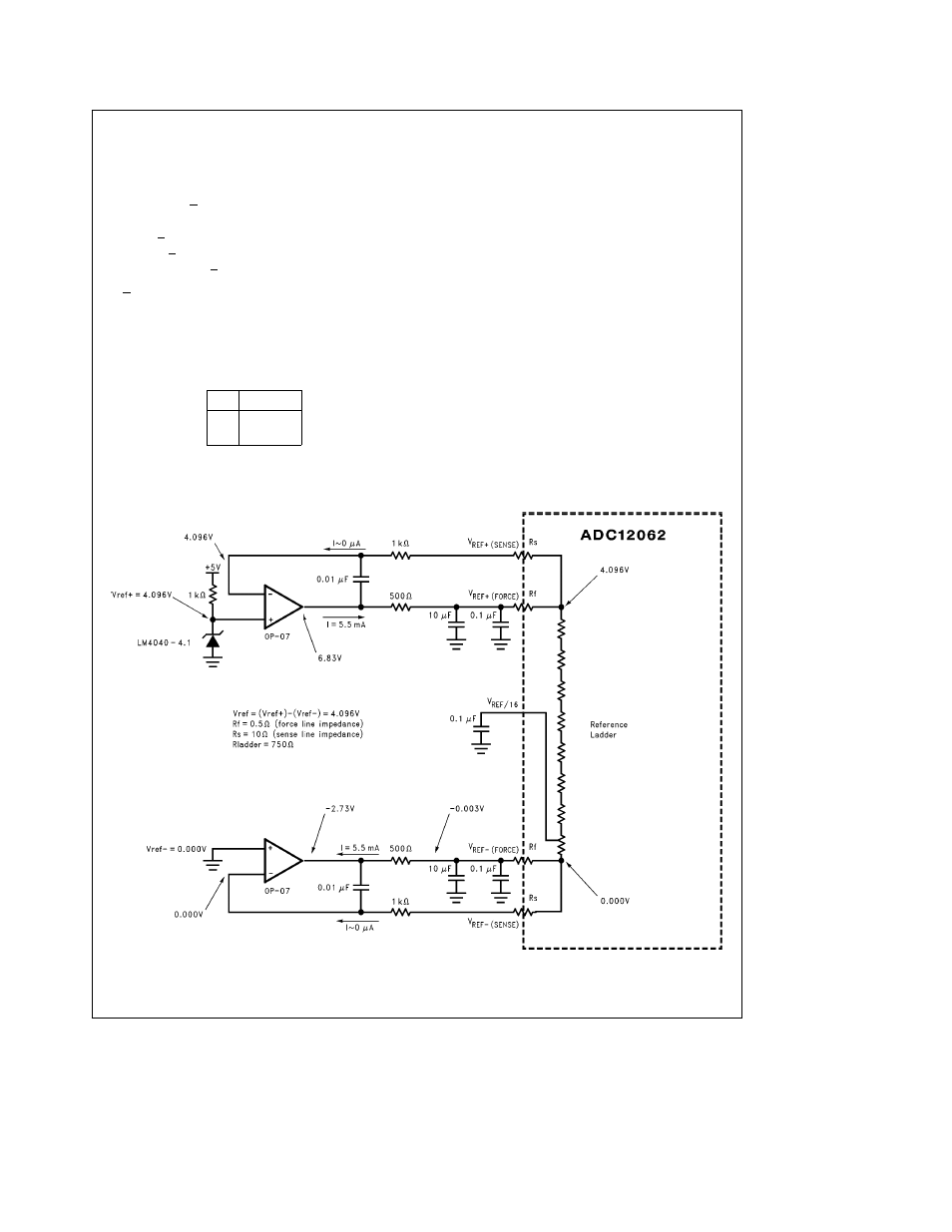
4 0 REFERENCE INPUTS
In addition to the fully differential V
REF
a
and V
REF
b
refer-
ence inputs used on most National Semiconductor ADCs
the ADC12062 has two sense outputs for precision control
of the ladder voltage These sense inputs compensate for
errors due to IR drops between the reference source and
the ladder itself The resistance of the reference ladder is
typically 750X The parasitic resistance (R
P
) of the package
leads bond wires PCB traces etc can easily be 0 5X to
1 0X or more This may not be significant at 8-bit or 10-bit
resolutions but at 12 bits it can introduce voltage drops
causing offset and gain errors as large as 6 LSBs
The ADC12062 provides a means to eliminate this error by
bringing out two additional pins that sense the exact voltage
at the top and bottom of the ladder With the addition of two
op amps the voltages on these internal nodes can be
forced to the exact value desired as shown in
Figure 10
TL H 11490 – 20
FIGURE 10 Reference Ladder Force and Sense Inputs
14
