Chip information, Pin configuration – Rainbow Electronics MAX17061 User Manual
Page 24
MAX17061
4) Place the overvoltage detection divider resistors as
close as possible to the OV pin. The divider’s cen-
ter trace should be kept short. Placing the resistors
far away causes the sensing trace to become
antennas that can pick up switching noise. Avoid
running the sensing traces near LX.
5) Place IN pin bypass capacitor as close as possible
to the device. The ground connection of the IN
bypass capacitor should be connected directly to
GND pins with a wide trace.
6) Minimize the size of the LX node while keeping it
wide and short. Keep the LX node away from the
feedback node and ground. If possible, avoid run-
ning the LX node from one side of the PCB to the
other. Use DC traces as shield if necessary.
Refer to the MAX17061 evaluation kit for an example of
proper board layout.
8-String White LED Driver with
SMBus for LCD Panel Applications
24
______________________________________________________________________________________
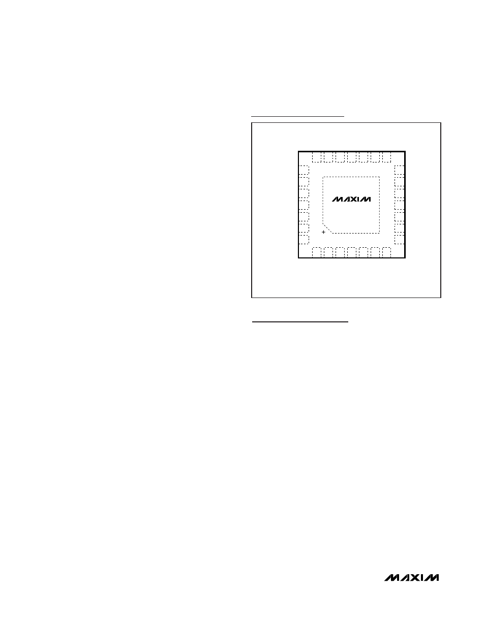
Chip Information
TRANSISTOR COUNT: 21,800
PROCESS: BiCMOS
26
27
25
24
10
9
11
FB4
N.C.
FB5
N.C.
FB6
12
FB3
PGND1
N.C.
LX1
IN
LX2
SCL
1
2
OV
4
5
6
7
20
21
19
17
16
15
ISET
FB1
PWMO
PWMI
OSC
FB8
MAX17061ETI+
GND
PGND2
3
18
28
8
FB2
FB7
CCV
23
13
FSET
V
CC
22
14
SDA
V
DD
TOP VIEW
THIN QFN
4mm x 4mm
Pin Configuration