Fixed-frequency step-up controller, Internal 5v linear regulator v, And uvlo – Rainbow Electronics MAX17061 User Manual
Page 12
MAX17061
The MAX17061 includes a 5V linear regulator that pro-
vides the internal bias and gate drive for the step-up
controller. When an external 5V is available, the internal
LDO can be overdriven to decrease power dissipation.
Otherwise, connect the IN pin to an input greater than 5.5V.
Fixed-Frequency Step-Up Controller
The MAX17061’s fixed-frequency, current-mode, step-
up controller automatically chooses the lowest active
FB_ voltage to regulate the output voltage. Specifically,
the difference between the lowest FB_ voltage and the
current-source control signal plus an offset (VSAT) is
integrated at the CCV output. The resulting error signal
is compared to the external switch current plus slope
compensation to determine the switch on-time. As the
load changes, the error amplifier sources or sinks cur-
rent to the CCV output to deliver the required peak-
inductor current. The slope-compensation signal is
added to the current-sense signal to improve stability at
high duty cycles.
When the input voltage is close to the output voltage, the
MAX17061 automatically skips pulses to prevent over-
charging the output capacitor. In SKIP mode, the induc-
tor current ramps up for a minimum on-time of
approximately 90ns, and then discharges the stored
energy to the output. The switch remains off until another
pulse is needed to boost the output voltage.
Internal 5V Linear Regulator
V
CC
and UVLO
The MAX17061 includes an internal low-dropout linear
regulator (V
CC
). When V
IN
is higher than 5.5V, this lin-
ear regulator generates a 5V supply to power internal
PWM controller, control logic, and MOSFET driver. The
V
CC
voltage drops to 4.35V in shutdown. If V
IN
is less
than or equal to 5.5V, V
CC
and IN can be tied together
and powered from an external 5V supply. There is an
internal diode from V
CC
to IN, so V
IN
must be greater
than V
CC
(see Figure 3).
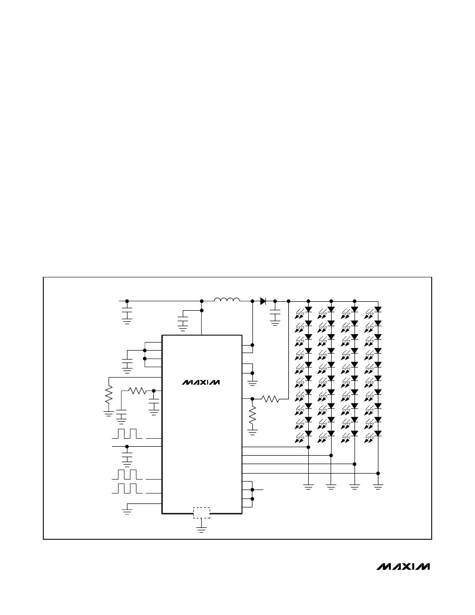
8-String White LED Driver with
SMBus for LCD Panel Applications
12
______________________________________________________________________________________
FB1
FSET
PGND2
PGND1
IN
V
IN
7V TO 21V
LX2
OV
FB2
FB3
FB4
FB5
FB6
FB7
FB8
L1
10
μH
0.1
μF
1
μF
1
μF
4.7
μF
D1
V
DD
OSC
GND
V
CC
PWMI
PWM
ISET
V
CC
C
OUT
LX1
MAX17061
V
OUT
UP TO 45V
220pF
464k
Ω
0.022
μF
5.1k
Ω
CCV
SCL
CLK
SDA
DATA
PWMO
EP
R2
61.9k
Ω
2
μF
R1
2.21M
Ω
Figure 1. Typical Operating Circuit