Rainbow Electronics MAX17061 User Manual
Page 18
MAX17061
8-String White LED Driver with
SMBus for LCD Panel Applications
18
______________________________________________________________________________________
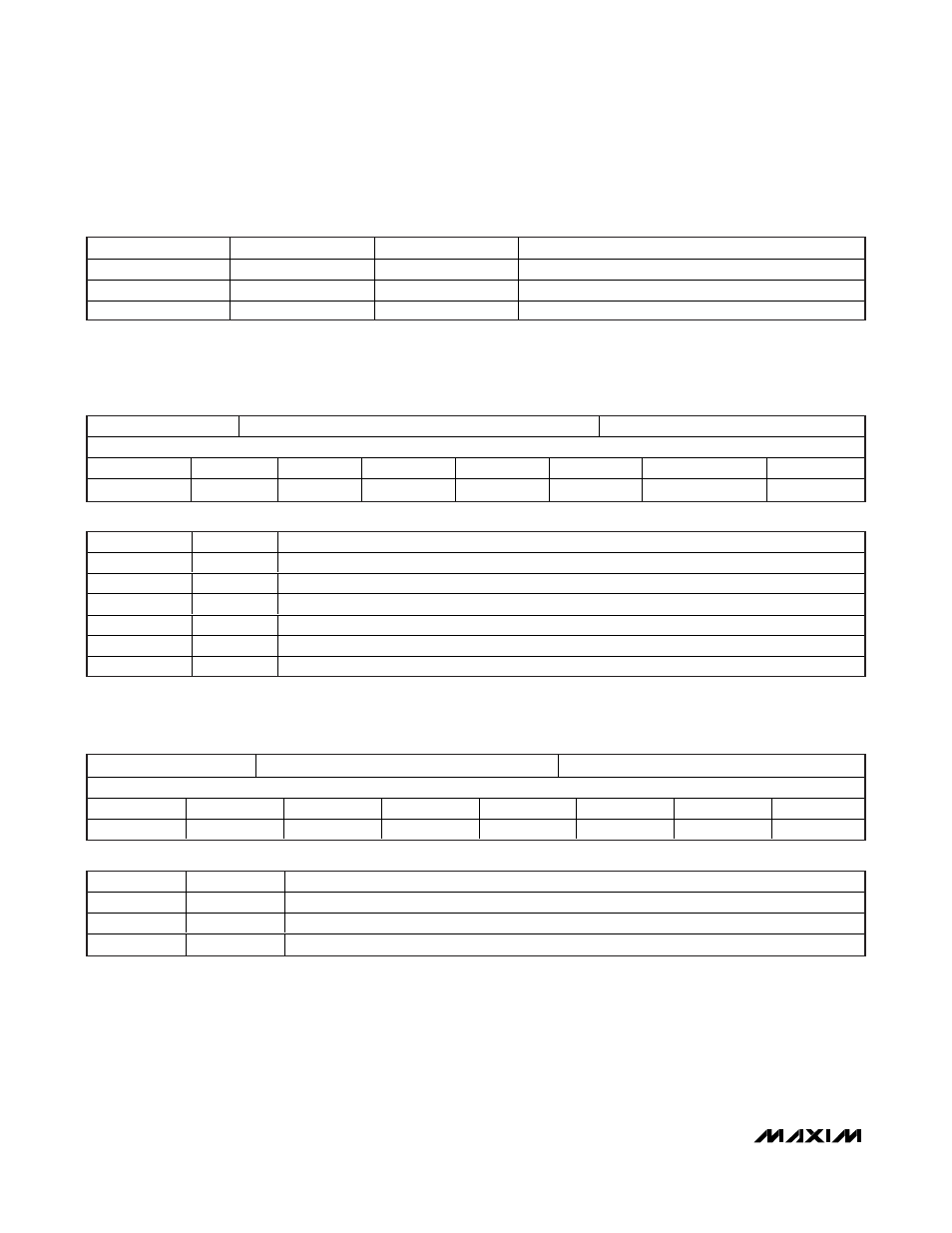
REGISTER 0x02
FAULT STATUS REGISTER
DEFAULT VALUE 0x00
RESERVED
RESERVED
2_CH_SD
1_CH_SD
BL_STAT
OV_CURR
THRM_SHDN
FAULT
Bit 7 (R)
Bit 6 (R)
Bit 5 (R)
Bit 4 (R)
Bit 3 (R)
Bit 2 (R)
Bit 1 (R)
Bit 0 (R)
BIT FIELD
DEFINITION
DESCRIPTION
Bit 5
2_CH_SD
Two or more LED output channels are faulted (1 = faulted, 0 = OK)
Bit 4
1_CH_SD
One LED output channel is faulted (1 = faulted, 0 = OK)
Bit 3
BL_STAT
Backlight status (1 = BL on, 0 = BL off)
Bit 2
OV_CURR
Input overcurrent (1 = overcurrent condition, 0 = current OK)
Bit 1
THRM_SHD
Thermal shutdown (1 = thermal fault, 0 = thermal OK)
Bit 0
FAULT
Any faul t excep t LE D op en/shor t occur s ( l og i c O R of al l faul t cond i ti ons, 1 = faul t cond i ti on, 0 = no faul t)
Fault/Status Register: Address is 0x02. This register has 6 status bits that allow monitoring the backlight con-
troller’s operating state. Bit 6 and Bit 7 are reserved bits, and Bit 3 is the status indicator or backlight. The other 5
bits are fault indicators. Bit 0 is a logical OR of all fault codes except LED open/short to simplify error detection. All
the bits in this register are read only. The reserved bits return a zero when read.
Bit field definitions:
REGISTER 0x03
ID REGISTER
DEFAULT VALUE 0x80
LED PANEL
MFG3
MFG2
MFG1
MFG0
REV2
REV1
REV0
Bit 7 = 1
Bit 6 (R)
Bit 5 (R)
Bit 4 (R)
Bit 3 (R)
Bit 2 (R)
Bit 1 (R)
Bit 0 (R)
BIT FIELD
DEFINITION
DESCRIPTION
Bit 7
LED panel
Display panel using LED backlight, bit 7 = 1
Bit [6..3]
MFG[3..0]
Manufacturer ID; see Table 3, default = 0
Bit [2..0]
REV[2..0]
Silicon rev (revs 0–7 allowed for silicon spins), default = 0
Identification Register: Address is 0x03. The ID register contains two bit fields to denote the manufacturer and the
silicon revision of the controller IC. The bit field widths were chosen to allow up to 32 vendors with up to eight silicon
revisions each. This register is read only.
Bit field definitions:
Table 2. Operating Modes Selected by Device Control Register Bits 1 and 2
PWM_MD
PWM_SEL
MODE
DPWM DUTY-CYCLE SETTING
X
1
PWM mode
PWMI input duty cycle
1
0
SMBus mode
SMBus command
0
0
DPST mode
Product of PWMI input duty cycle and SMBus command