Rainbow Electronics MAX17061 User Manual
Page 2
ABSOLUTE MAXIMUM RATINGS
ELECTRICAL CHARACTERISTICS
(Circuit of Figure 1, V
IN
= 12V, C
CCV
= 0.022µF, R
CCV
= 5.1k
Ω, V
ISET
= V
OSC
= V
DD
= V
CC
, R
FSET
= 464k
Ω, V
PWMI
= GND,
T
A
= 0°C to +85°C, unless otherwise noted. Typical values are at T
A
= +25°C.)
Stresses beyond those listed under “Absolute Maximum Ratings” may cause permanent damage to the device. These are stress ratings only, and functional
operation of the device at these or any other conditions beyond those indicated in the operational sections of the specifications is not implied. Exposure to
absolute maximum rating conditions for extended periods may affect device reliability.
IN to GND ..............................................................-0.3V to +28V
FB_, LX_ to GND ....................................................-0.3V to +45V
PGND_ to GND......................................................-0.3V to +0.3V
V
CC
, V
DD
, PWMI, SDA, SCL to GND ........................-0.3V to +6V
ISET, CCV, PWMO, FSET, OSC,
OV to GND ................................................-0.3V to V
CC
+ 0.3V
Continuous Power Dissipation (T
A
= +70°C)
28-Pin Thin QFN (derate 16.9mW/°C above +70°C) ...1667mW
Operating Temperature Range ...........................-40°C to +85°C
Junction Temperature ......................................................+150°C
Storage Temperature Range .............................-60°C to +150°C
Lead Temperature (soldering, 10s) .................................+300°C
MAX17061
8-String White LED Driver with
SMBus for LCD Panel Applications
2
_______________________________________________________________________________________
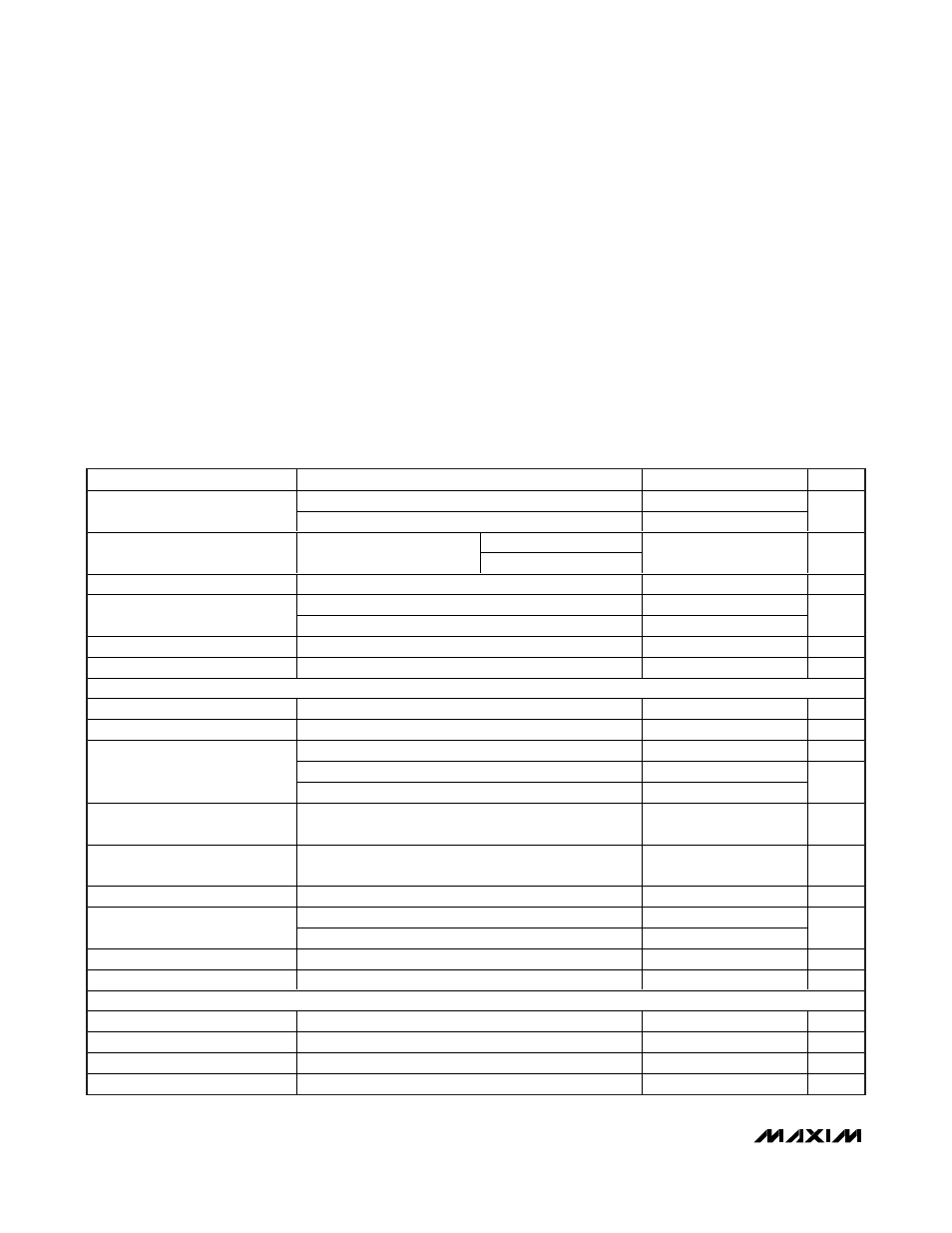
PARAMETER
CONDITIONS
MIN
TYP
MAX
UNITS
V
IN
= V
CC
4.5
5.5
IN Input Voltage Range
V
CC
= open
5.5
26.0
V
V
IN
= 26V
IN Quiescent Current
MAX17061 is enabled at
minimum brightness, no load
V
IN
= V
CC
= 5V
1.24
2
mA
IN Quiescent Current
MAX17061 is disabled, V
I N
= 12V
10
µA
M AX 17061 i s enab l ed , 6V < V
I N
< 26V , 0 < I
V C C
< 10m A
4.7
5.0
5.3
V
CC
Output Voltage
MAX17061 is disabled, V
I N
=
12V
3.90
4.35
4.80
V
V
CC
Current Limit
V
C C
is forced to 4.5V
15
40
70
mA
V
CC
UVLO Threshold
Rising edge, typical hysteresis = 85mV
4.00
4.25
4.45
V
BOOST CONVERTER
LX On-Resistance
20mA from LX_ to PGND
0.15
0.3
Ω
LX Leakage Current
45V on LX_
1
µA
V
OSC
= V
CC
0.9
1.0
1.1
MHz
V
OSC
= open
675
750
825
Operating Frequency
V
OSC
= GND
450
500
550
kHz
OSC High-Level Threshold
V
CC
-
0.4
V
OSC Midlevel Threshold
1.5
V
CC
-
2.0
V
OSC Low-Level Threshold
0.4
V
PWM mode (Note 1)
10
Minimum Duty Cycle
Pulse skipping, no load (Note 1)
0
%
Maximum Duty Cycle
94.0
95.5
97.0
%
LX Current Limit
Duty cycle = 75% (Note 1)
1.6
A
CONTROL INPUT
SDA, SCL Logic Input-High Level
2.1
V
SDA, SCL Logic Input-Low Level
0.8
V
PWMI Logic Input-High Level
2.1
V
PWMI Logic Input-Low Level
0.8
V