Electrical characteristics (continued) – Rainbow Electronics MAX17036 User Manual
Page 5
MAX17030/MAX17036
1/2/3-Phase Quick-PWM
IMVP-6.5 VID Controllers
_______________________________________________________________________________________
5
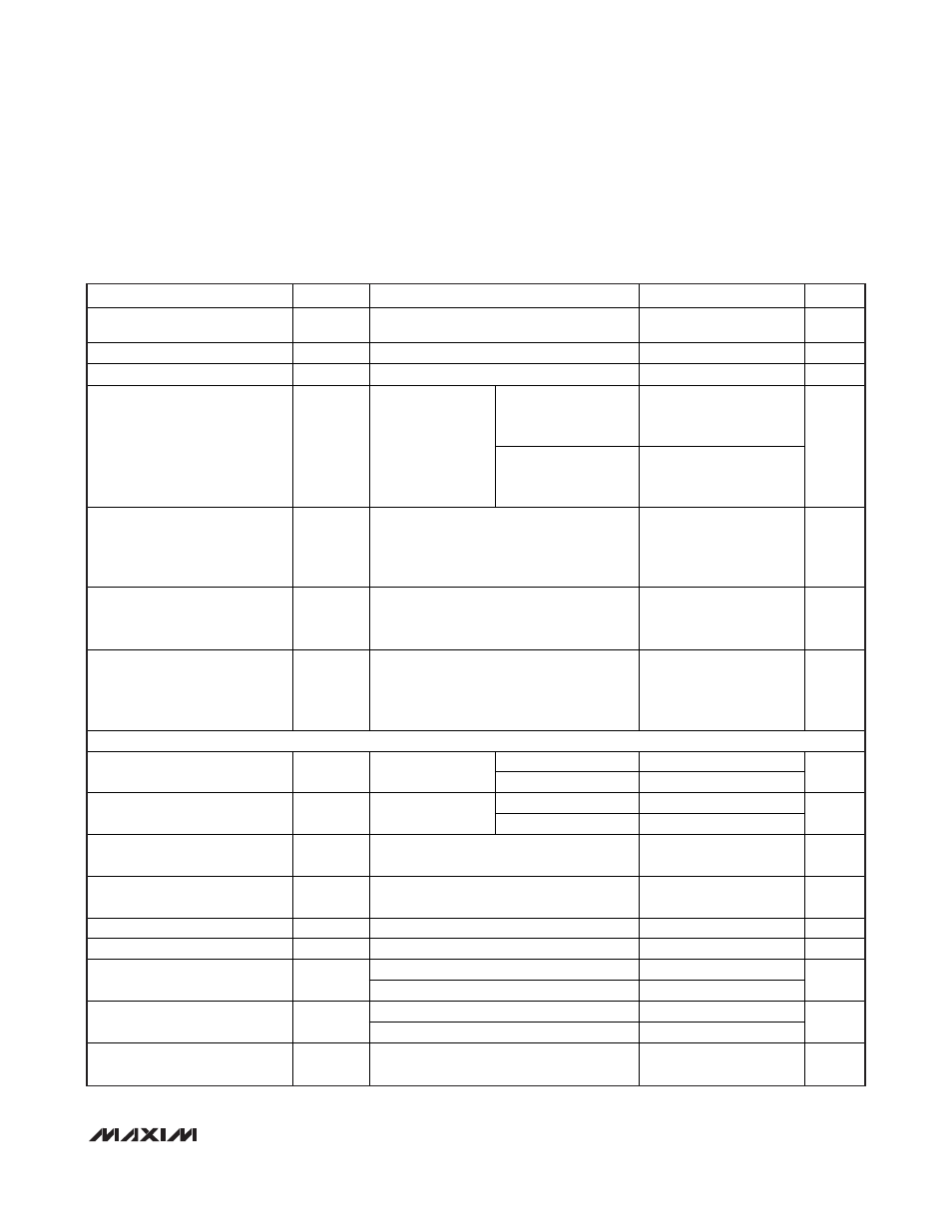
ELECTRICAL CHARACTERISTICS (continued)
(Circuit of Figure 1, V
IN
= 10V, V
CC
= V
DD
= V
SHDN
= V
PGD_IN
= V
PSI
= V
ILIM
= 5V, V
DPRSLPVR
= V
GNDS
= 0, V
CSP_
= V
CSN_
=
1.0000V, FB = FBAC, R
FBAC
= 3.57k
Ω from FBAC to CSN_, [D6–D0] = [0101000]; T
A
= 0°C to +85°C, unless otherwise noted.
Typical values are at T
A
= +25°C.)
PARAMETER SYMBOL
CONDITIONS
MIN
TYP
MAX
UNITS
Phases 2, 3 Disable Threshold
Measured at CSP2, CSP3
3
V
CC
-
1
V
CC
-
0.4
V
CSP_, CSN_ Input Current
I
CSP
, I
CSN
T
A
= +25
°C -0.2
+0.2
μA
ILIM Input Current
I
ILIM
T
A
= +25
°C -0.1
+0.1
μA
T
A
= +25°C
-0.5
+0.5
Droop Amplifier Offset
(1/N) x
(V
CSP_
-
V
CSN_
) at I
FBAC
= 0;
indicates
summation over all
power-up enabled
phases from 1 to N,
N = 3
T
A
= 0
°C to +85°C
-0.75
+0.75
mV/
phase
Droop Amplifier
Transconductance
G
m(FBAC)
I
FBAC
/
[(V
CSP_
- V
CSN_
)];
indicates summation over all power-up
enabled phases from 1 to N, N = 3,
V
FBAC
= V
CSN_
= 0.45V to 1.5V
393 400 406 μS
Current-Monitor Offset
(1/N) x
(V
CSP_
- V
CSN_
) at I
IMON
= 0,
indicates summation over all power-up
enabled phases from 1 to N, N = 3
-1.1 +1
mV/
phase
Current-Monitor
Transconductance
G
m(IMON)
I
IMON
/
[(V
CSP_
- V
CSN_
)];
indicates summation over all power-up
enabled phases from 1 to N, N = 3,
V
CSN_
= 0.45V to 1.5V
1.552 1.6 1.648 mS
GATE DRIVERS
High state (pullup)
0.9
2.5
DH_ Gate-Driver On-Resistance
R
ON(DH)
BST_ - LX_ forced
to 5V
Low state (pulldown)
0.7
2
High state (pullup)
0.7
2
DL_ Gate-Driver On-Resistance
R
ON(DL)
Low
state
(pulldown) 0.25
0.7
DH_ Gate-Driver Source Current
I
DH(SOURCE)
DH_ forced to 2.5V,
BST_ - LX_ forced to 5V
2.2 A
DH_ Gate-Driver Sink Current
I
DH(SINK)
DH_ forced to 2.5V,
BST_ - LX_ forced to 5V
2.7 A
DL_ Gate-Driver Source Current
I
DL(SOURCE)
DL_ forced to 2.5V
2.7
A
DL_ Gate-Driver Sink Current
I
DL(SINK)
DL_ forced to 2.5V
8
A
DL_ falling, C
DL_
=
3nF
20
DL_ Transition Time
DL rising, C
DL_
=
3nF
20
ns
DH_ falling, C
DH_
= 3nF
20
DH_ Transition Time
DH_ rising, C
DH_
=
3nF
20
ns
Internal BST_ Switch
On-Resistance
R
ON(BST)
I
BST_
= 10mA
10
20