Multiphase quick-pwm design procedure – Rainbow Electronics MAX17036 User Manual
Page 33
MAX17030/MAX17036
1/2/3-Phase Quick-PWM
IMVP-6.5 VID Controllers
______________________________________________________________________________________
33
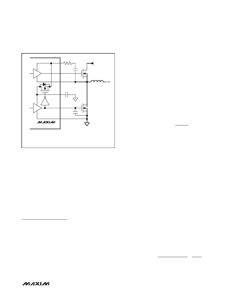
Shoot-through currents can also be caused by a com-
bination of fast high-side MOSFETs and slow low-side
MOSFETs. If the turn-off delay time of the low-side
MOSFET is too long, the high-side MOSFETs can turn
on before the low-side MOSFETs have actually turned
off. Adding a resistor less than 5
Ω in series with BST
slows down the high-side MOSFET turn-on time, elimi-
nating the shoot-through currents without degrading the
turn-off time (R
BST
in Figure 10). Slowing down the
high-side MOSFET also reduces the LX node rise time,
thereby reducing EMI and high-frequency coupling
responsible for switching noise.
Multiphase Quick-PWM
Design Procedure
Firmly establish the input voltage range and maximum
load current before choosing a switching frequency and
inductor operating point (ripple-current ratio). The pri-
mary design trade-off lies in choosing a good switching
frequency and inductor operating point, and the following
four factors dictate the rest of the design:
•
Input voltage range: The maximum value
(V
IN(MAX)
) must accommodate the worst-case high
AC adapter voltage. The minimum value (V
IN(MIN)
)
must account for the lowest input voltage after
drops due to connectors, fuses, and battery selec-
tor switches. If there is a choice at all, lower input
voltages result in better efficiency.
•
Maximum load current: There are two values to
consider. The peak load current (I
LOAD(MAX)
) deter-
mines the instantaneous component stresses and
filtering requirements, and thus drives output
capacitor selection, inductor saturation rating, and
the design of the current-limit circuit. The continu-
ous load current (I
LOAD
) determines the thermal
stresses and thus drives the selection of input
capacitors, MOSFETs, and other critical heat-con-
tributing components. Modern notebook CPUs gen-
erally exhibit I
LOAD
= I
LOAD(MAX)
x 80%.
For multiphase systems, each phase supports a
fraction of the load, depending on the current bal-
ancing. When properly balanced, the load current is
evenly distributed among each phase:
where η
TOTAL
is the total number of active phases.
•
Switching frequency: This choice determines the
basic trade-off between size and efficiency. The
optimal frequency is largely a function of maximum
input voltage, due to MOSFET switching losses that
are proportional to frequency and V
IN
2
. The opti-
mum frequency is also a moving target, due to
rapid improvements in MOSFET technology that are
making higher frequencies more practical.
•
Inductor operating point: This choice provides
trade-offs between size vs. efficiency and transient
response vs. output noise. Low inductor values pro-
vide better transient response and smaller physical
size, but also result in lower efficiency and higher
output noise due to increased ripple current. The
minimum practical inductor value is one that causes
the circuit to operate at the edge of critical conduc-
tion (where the inductor current just touches zero
with every cycle at maximum load). Inductor values
lower than this grant no further size-reduction bene-
fit. The optimum operating point is usually found
between 30% and 50% ripple current. for a multi-
phase core regulator, select an LIR value of ~0.4.
Inductor Selection
The switching frequency and operating point (% ripple
current or LIR) determine the inductor value as follows:
where η
TOTAL
is the total number of phases.
L
V
V
f
I
LIR
V
V
TOTAL
IN
OUT
SW LOAD MAX
OUT
=
−
⎛
⎝
⎜
⎞
⎠
⎟
η
(
)
IIN
⎛
⎝⎜
⎞
⎠⎟
I
I
LOAD PHASE
LOAD
TOTAL
(
)
=
η
BST_
DH_
LX_
(R
BST
)*
INPUT (V
IN
)
C
BST
N
H
C
BYP
L
(R
BST
)* OPTIONAL—THE RESISTOR LOWERS EMI BY DECREASING THE
SWITCHING NODE RISE TIME.
(C
NL
)* OPTIONAL—THE CAPACITOR REDUCES LX TO DL CAPACITIVE
COUPLING THAT CAN CAUSE SHOOT-THROUGH CURRENT.
DL_
PGND
N
L
(C
NL
)*
V
DD
MAX17030/MAX17036
Figure 10. Gate Drive Circuit