Absolute maximum ratings, Electrical characteristics – Rainbow Electronics MAX17036 User Manual
Page 2
MAX17030/MAX17036
1/2/3-Phase Quick-PWM
IMVP-6.5 VID Controllers
2
_______________________________________________________________________________________
ABSOLUTE MAXIMUM RATINGS
(Note 1)
ELECTRICAL CHARACTERISTICS
(Circuit of Figure 1, V
IN
= 10V, V
CC
= V
DD
= V
SHDN
= V
PGD_IN
= V
PSI
= V
ILIM
= 5V, V
DPRSLPVR
= V
GNDS
= 0, V
CSP_
= V
CSN_
=
1.0000V, FB = FBAC, R
FBAC
= 3.57k
Ω from FBAC to CSN_, [D6–D0] = [0101000]; T
A
= 0°C to +85°C, unless otherwise noted.
Typical values are at T
A
= +25°C.)
Stresses beyond those listed under “Absolute Maximum Ratings” may cause permanent damage to the device. These are stress ratings only, and functional
operation of the device at these or any other conditions beyond those indicated in the operational sections of the specifications is not implied. Exposure to
absolute maximum rating conditions for extended periods may affect device reliability.
V
CC
, V
DD
to GND .....................................................-0.3V to +6V
D0–D6, PGD_IN, PSI, DPRSLPVR to GND ...............-0.3V to +6V
CSP_, CSN_, THRM, ILIM to GND............................-0.3V to +6V
PWRGD, CLKEN, VR_HOT to GND..........................-0.3V to +6V
FB, FBAC, IMON, TIME to GND .................-0.3V to (V
CC
+ 0.3V)
SHDN to GND (Note 2)...........................................-0.3V to +30V
TON to GND ...........................................................-0.3V to +30V
GNDS to GND .......................................................-0.3V to +0.3V
DL1, DL2, PWM3, DRSKP to GND .............-0.3V to (V
DD
+ 0.3V)
BST1, BST2 to GND ...............................................-0.3V to +36V
BST1, BST2 to V
DD
.................................................-0.3V to +30V
LX1 to BST1..............................................................-6V to +0.3V
LX2 to BST2..............................................................-6V to +0.3V
DH1 to LX1 ..............................................-0.3V to (V
BST1
+ 0.3V)
DH2 to LX2 ..............................................-0.3V to (V
BST2
+ 0.3V)
Continuous Power Dissipation (40-pin, 5mm x 5mm TQFN)
Up to +70°C ..............................................................1778mW
Derating above +70°C ..........................................22.2mW/°C
Operating Temperature Range .........................-40°C to +105°C
Junction Temperature ......................................................+150°C
Storage Temperature Range .............................-65°C to +165°C
Lead Temperature (soldering, 10s) .................................+300°C
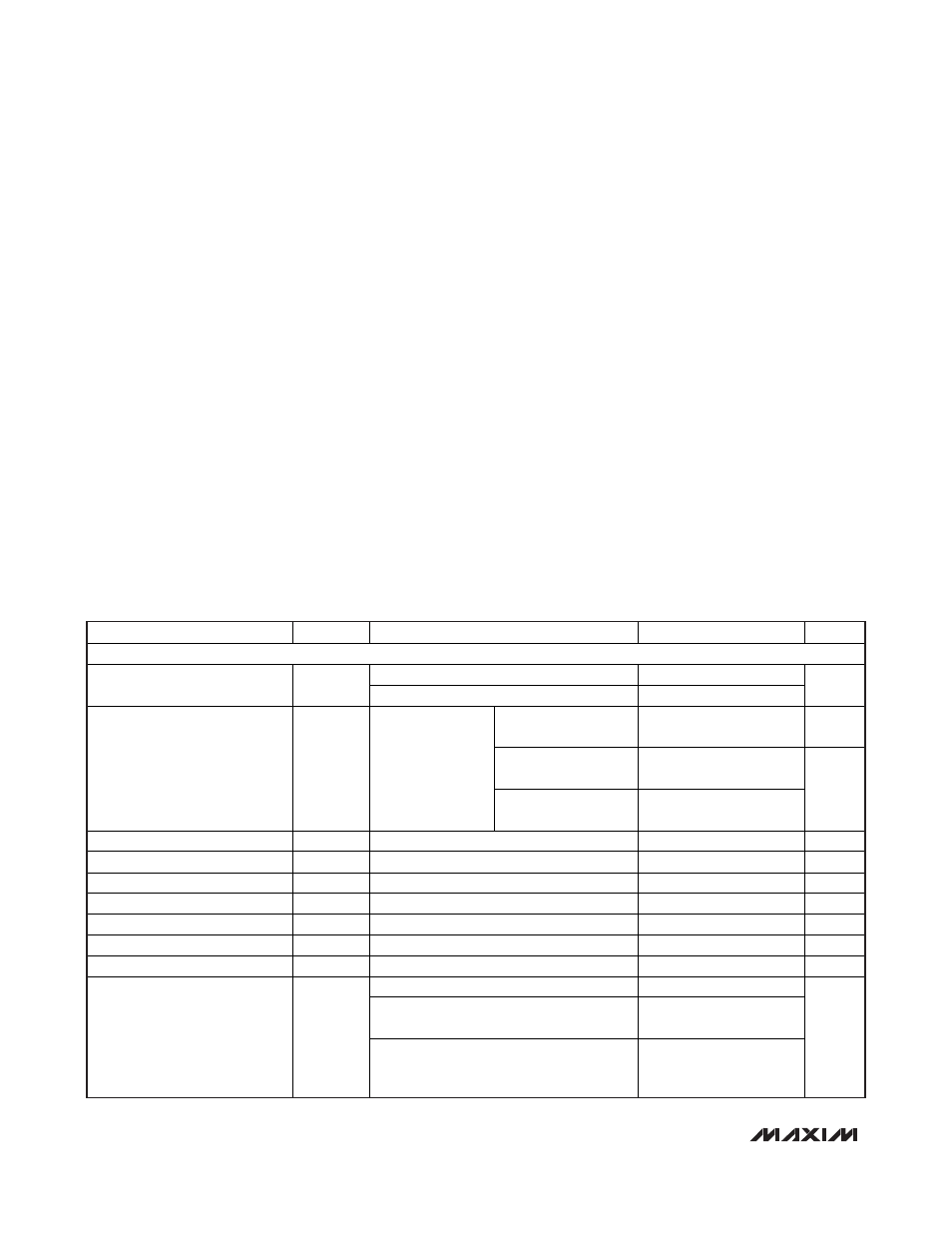
PARAMETER
SYMBOL
CONDITIONS
MIN
TYP
MAX
UNITS
PWM CONTROLLER
V
CC
, V
DD
4.5 5.5
Input Voltage Range
V
IN
7
26
V
DAC codes from
0.8125V to 1.5000V
-0.5 +0.5 %
DAC codes from
0.3750V to 0.8000V
-7 +7
FB Output Voltage Accuracy
V
FB
Measured at FB
with respect to
GNDS;
includes load-
regulation error
(Note 3)
DAC codes from
0 to 0.3625V
-20 +20
mV
Boot Voltage
V
BOOT
1.094
1.100
1.106
V
Line Regulation Error
V
CC
= 4.5V to 5.5V, V
IN
= 4.5V to 26V
0.1
%
FB Input Bias Current
T
A
= +25
°C -0.1
+0.1
µA
GNDS Input Range
-200
+200
mV
GNDS Gain
A
GNDS
V
OUT
/
V
GNDS
0.97 1.00 1.03 V/V
GNDS Input Bias Current
I
GNDS
T
A
= +25
°C -0.5
+0.5
µA
TIME Regulation Voltage
V
TIME
R
TIME
= 147k
1.985
2.000
2.015
V
R
TIME
= 147k
(6.08mV/µs nominal)
-10
+10
R
TIME
= 35.7k
(25mV/µs nominal) to
178k
(5mV/µs nominal)
-15 +15
TIME Slew-Rate Accuracy
Soft-start and soft-shutdown:
R
TIME
= 35.7k
(6.25mV/µs nominal) to
178k
(1.25mV/µs nominal)
-20 +20
%
Note 1: Absolute Maximum Ratings valid using 20MHz bandwidth limit.
Note 2: SHDN might be forced to 12V for the purpose of debugging prototype breadboards using the no-fault test mode. Internal
BST switches are disabled as well. Use external BST diodes when SHDN is forced to 12V.