Step immunity and no r, Sense – Rainbow Electronics MAX5937 User Manual
Page 8
MAX5936/MAX5937
-48V Hot-Swap Controllers with V
IN
Step Immunity and No R
SENSE
8
_______________________________________________________________________________________
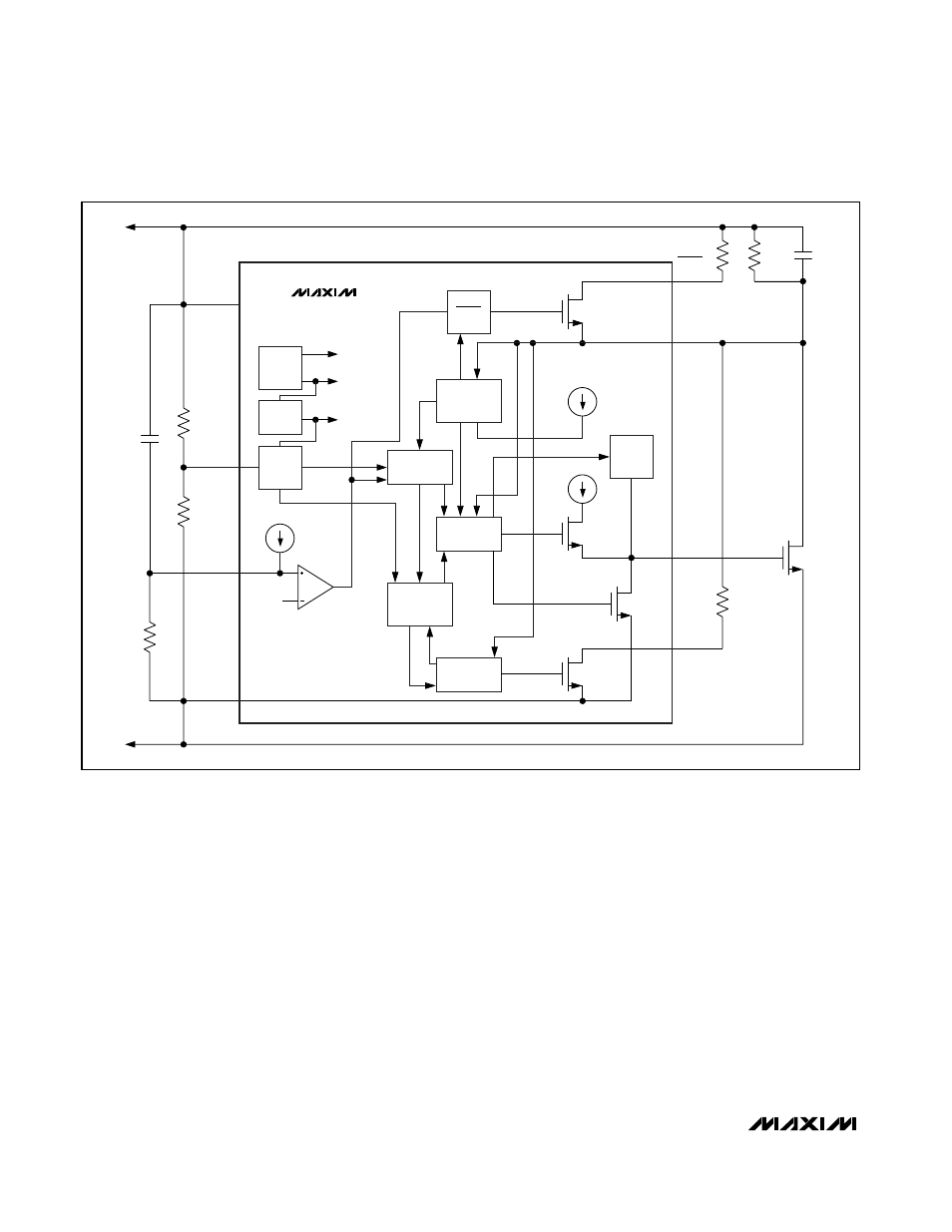
The MAX5936/MAX5937 conduct a load-probe test after
contact transients from the hot plug-in have settled. This
follows the MAX5936/MAX5937 power-up (when the
UVLO condition has been met for 220ms (t
LP
)) and prior
to the turn-on of the power MOSFET. This test pulls a
user-programmable current through the load (1A, max)
for up to 220ms and tests for a voltage of 200mV across
the load at V
OUT
. This current is set by an external resis-
tor, R
LP
, between V
OUT
and LP (Figure 14). When the
voltage across the load exceeds 200mV, the test is trun-
cated and the GATE turn-on sequence is started. If at the
end of the 220ms test period the voltage across the load
has not reached 200mV, the load is assumed to be short-
ed and the current to the load from the LP pin is shut off.
The MAX5936A_/MAX5937A_ will timeout for 16 x t
LP
then retry the load-probe test. The MAX5936L_/
MAX5937L_ will latch the fault condition indefinitely until
the UVLO is brought below 1.125V for 1.5ms or the power
is recycled. See the Applications Information section for
recommendations on selecting R
LP
to set the current
level.
Upon successful completion of the load-probe test, the
MAX5936/MAX5937 enter the power-up GATE cycle and
begin ramping the GATE voltage with a 52µA current
source. This current source is restricted if V
OUT
begins
to ramp down faster than the default 9V/ms slew rate.
Charging up GATE enhances the power MOSFET in a
controlled manner and ramping V
OUT
at a user-settable
rate controls the inrush current from the backplane. The
MAX5936/MAX5937 continue to charge up the GATE
until one of two events occurs: a normal power-up GATE
cycle is completed or a power-up to fault management is
detected (see the GATE Cycles section in Appendix A).
Figure 1. Functional Block Diagram
10V REG
AND
5V REG
UVLO
LOGIC
CONTROL
BANDGAP
REF
V
BG
10µA
FAULT
DETECTION
SEQUENCER
CONTROLLER
TIMER
GATE
CONTROL
LOAD PROBE
TEST
V
SC
, V
CB
, AND
75% OF V
CB
COMPARATORS
STEP
TEMPERATURE-
COMPENSATED
CURRENT SOURCE
V
BG
(1.25V)
+5V
+10V
52µA
2V AND
15V
CLAMP
PGOOD
PGOOD
LOGIC
MAX5936
MAX5937
PGOOD
PGOOD
V
OUT
GATE
LP
R
LOAD
C
LOAD
UVLO
GND
STEP_MON
V
EE
GND
V
EE