Step immunity and no r, Sense – Rainbow Electronics MAX5937 User Manual
Page 14
MAX5936/MAX5937
-48V Hot-Swap Controllers with V
IN
Step Immunity and No R
SENSE
14
______________________________________________________________________________________
This occurs with the least possible disturbance to V
OUT
,
although during the brief period that the MOSFET is off,
the voltage across the load droops slightly depending
on the load current and load storage capacitance.
PGOOD remains asserted throughout the V
IN
step
event.
The objective in selecting the resistor and capacitor for
the step monitor function is to ensure that the V
IN
steps
of all anticipated slopes and magnitudes will be proper-
ly detected and blocked, which otherwise would result
in a circuit-breaker or short-circuit fault. The following is
a brief analysis for finding the resistor and capacitor.
For a more complete analysis, see Appendix B.
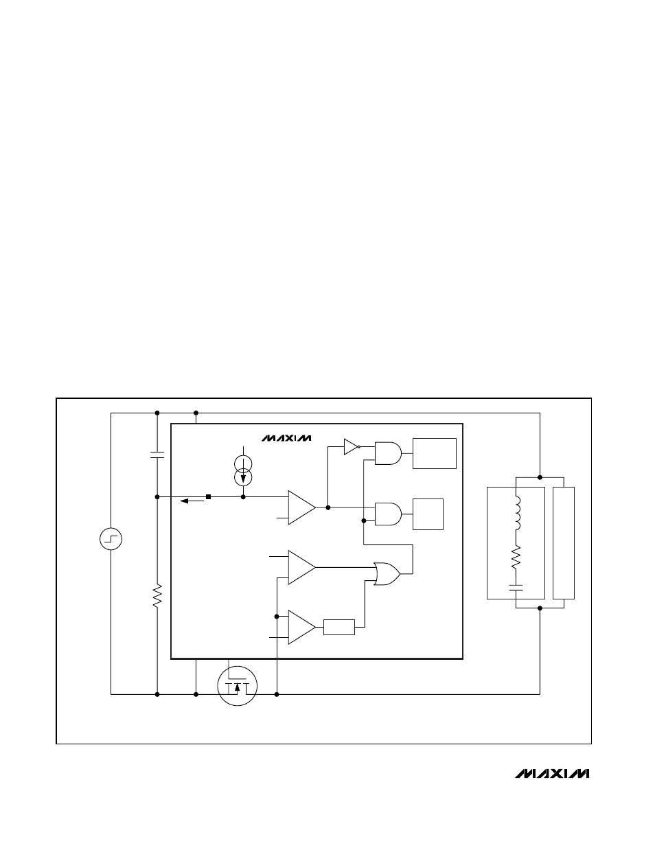
Figure 13 is a functional diagram exhibiting the
elements of the MAX5936/MAX5937 involved in the
step immunity function. This block diagram shows the
parallel relationship between V
OUT
and V
STEP-MON
.
Each has an I*R component establishing the DC level
prior to a step. While it is referred to as a V
IN
step, it is
the dynamic response to a finite voltage ramp that is
of interest.
Given a positive V
IN
ramp with a ramp rate of dV/dt, the
approximate response of V
OUT
to V
IN
is:
V
OUT
(t) = (dV/dt) x τ
C
x (1-e
(-t / τ
L
,eqv)
)
+ R
DS(ON)
x I
LOAD
where τ
C
= C
LOAD
x R
DS(ON)
and τ
L
,eqv is the equiva-
lent time constant of the load that must be found empir-
ically (see Appendix B).
Similarly, the response of STEP_MON to a V
IN
ramp is:
V
STEP_MON
(t) = (dV/dt) x τ
STEP
x (1-e
(-t / τSTEP)
) + 10µA
x R
STEP
where τ
STEP
= R
STEP_MON
x C
STEP_MON
.
For proper step detection, V
STEP_MON
must exceed
STEP
TH
prior to V
OUT
reaching V
SC
or within 1.4ms of
V
OUT
reaching V
CB
(overall V
IN
ramp rates anticipated in
the application). V
STEP_MON
must be set below STEP
TH
with adequate margin, ∆V
STEP_MON
, to accommodate
the tolerance of both I
STEP_OS
(±8%) and R
STEP_MON
.
R
STEP_MON
is typically set to 100kΩ which gives a
∆V
STEP_MON
for a worst-case high of 0.36V.
Figure 13. MAX5936/MAX5937 Step Immunity Functional Diagram
FAULT
MANAGEMENT
CYCLE
GATE
LOW
t
CB_DLY
ESL
ESR
C
LOAD
C
LOAD
C
STEP_MON
R
STEP_MON
V
STEP_MON
R
DS,ON
GATE
V
EE
V
OUT
V
IN
STEP
STEP_MON
I
STEP
I
STEP_OS
GND
STEP
TH
STEP_DET
V
SC
V
CB
CB TRIP
MAX5936
MAX5937
SC TRIP
NOTE: V
SC
, V
CB
, V
STEPTH
, V
STEP_MON
, AND VOUT ARE REFERENCED TO V
EE
.