Step immunity and no r, Sense, Pgood – Rainbow Electronics MAX5937 User Manual
Page 12
MAX5936/MAX5937
-48V Hot-Swap Controllers with V
IN
Step Immunity and No R
SENSE
12
______________________________________________________________________________________
PGOOD (
PGOOD
) Open-Drain Output
The power-good outputs, PGOOD (PGOOD), are open
drain and are referenced to V
OUT
. They assert and latch
if V
OUT
ramps below 72% of V
CB
, and with the built-in
delay this occurs 1.26ms after the external MOSFET
becomes fully enhanced. PGOOD (PGOOD) deasserts
any time the part enters fault management. PGOOD
(PGOOD) has a delayed response to UVLO. The GATE
goes to V
EE
when UVLO is brought below 1.125V for
1.5ms. This turns off the power MOSFET and allows
V
OUT
to rise depending on the RC time constant of the
load. PGOOD (PGOOD), in this situation, deasserts
when V
OUT
rises above V
CB
for more than 1.4ms or
above V
SC
, whichever occurs first (see Figure 12b).
Due to the open-drain driver, PGOOD (PGOOD)
requires an external pullup resistor to GND. Due to this
external pullup, PGOOD will not follow positive V
IN
steps as well as if it were driven by an active pullup. As
a result, when PGOOD (PGOOD) is asserted high, an
apparent negative glitch appears at PGOOD (PGOOD)
during a positive V
IN
step. This negative glitch is a
result of the RC time constant of the external resistor
and the PGOOD pin capacitance lagging the V
IN
step.
It is not due to switching of the internal logic. To mini-
mize this negative transient, it may be necessary to
increase the pullup current and/or to add a small
amount of capacitance from PGOOD (PGOOD) to GND
to compensate for the pin capacitance.
WARNING:
For the MAX5936_N/MAX5937_N, PGOOD
(PGOOD) asserts 1.26ms after the power MOSFET is fully
enhanced, independent of V
OUT
. Once the MOSFET is
fully enhanced and UVLO is pulled below its respective
threshold, GATE pulls to V
EE
to turn off the power
MOSFET and disconnect the load. When UVLO is
cycled low, PGOOD (PGOOD) remains asserted even
when V
OUT
has risen to GND and there is no voltage
across the load. In summary, once the MOSFET is fully
enhanced, the MAX5936_N/ MAX5937_N ignore V
OUT
and deassert PGOOD (PGOOD) only when the power
to the MAX5936_N/ MAX5937_N is fully recycled.
Undervoltage Lockout (UVLO)
UVLO provides an accurate means to set the turn-on volt-
age level for the MAX5936/MAX5937. Use a resistor-
divider network from GND to V
EE
to set the desired
turn-on voltage (Figure 11). UVLO has hysteresis with a
rising threshold of 1.25V and a falling threshold of 1.125V.
A startup delay of 220ms allows contacts and voltages to
settle prior to initiating the startup sequence (Figure 12a).
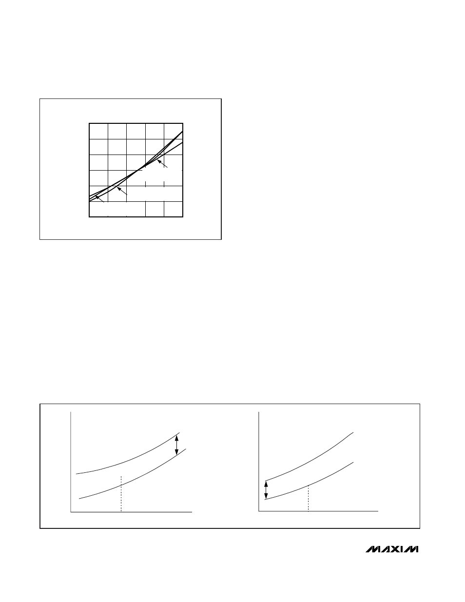
Figure 9. MAX5936/MAX5937 Normalized Circuit-Breaker
Threshold (V
CB
)
NORMALIZED MOSFET ON-RESISTANCE
vs. TEMPERATURE
TEMPERATURE (°C)
NORMALIZED MOSFET ON-RESISTANCE
60
35
10
-15
0.6
0.8
1.0
1.2
1.4
1.6
0.4
-40
85
IRF1310NS
NORMALIZED R
ON
IRFR3910
NORMALIZED R
ON
MAX5936/MAX5937
NORMALIZED V
CB
Figure 10. Circuit-Breaker Voltage Margin for High and Low Tempco Power MOSFETS
CIRCUIT-BREAKER
TRIP REGION
CIRCUIT-BREAKER
TRIP REGION
T
A
= +25°C
T
A
= +25°C
V
CB
I
D
x R
DS,ON
∆V
CB,MIN
∆V
CB,MIN
V
CB
I
D
x R
DS,ON
R
DS(ON)
HIGH TEMPCO
R
DS(ON)
LOW TEMPCO
VOL
TAGE
TEMPERATURE
TEMPERATURE
VOL
TAGE