Step immunity and no r, Sense – Rainbow Electronics MAX5937 User Manual
Page 16
MAX5936/MAX5937
-48V Hot-Swap Controllers with V
IN
Step Immunity and No R
SENSE
16
______________________________________________________________________________________
Adjusting the V
OUT
Slew Rate
The default slew rate is set internally for 9V/ms. The
slew rate can be reduced by placing an external
capacitor from the drain of the power MOSFET to the
GATE output of the MAX5936/MAX5937. Figure 15
shows a graph of Slew Rate vs. C
SLEW
. This graph
shows that for C
SLEW
< 4700pF there is very little effect
to the addition of external slew-rate control capaci-
tance. This is intended so the GATE output can drive
large MOSFETs with significant gate capacitance and
still achieve the default slew rate. To select a slew-rate
control capacitor, go into the graph with the desired
slew rate and find the value of the miller capacitance.
When C
SLEW
> 4700pF, SR and C
SLEW
are inversely
related. Given the desired slew rate, the required
C
SLEW
is found as follows:
C
SLEW
(nF) = 23 / SR (V/ms)
From the data sheet of the power MOSFET find the
reverse transfer capacitance (gate-to-drain capacitance)
above 10V. If the reverse transfer capacitance of the
external power MOSFET is 5% or more of C
SLEW
, then it
should be subtracted from C
SLEW
in the equation above.
Figure 16 gives an example of the external circuit for
controlling slew rate. Depending on the parasitics asso-
ciated with the selected power MOSFET, the addition of
C
SLEW
may lead to oscillation while the MOSFET and
GATE control are in the linear range. If this is an issue, an
external resistor, R
GATE
, in series with the gate of the
MOSFET is recommended to prevent possible oscilla-
tion. It should be as small as possible, e.g., 5Ω to 10Ω, to
avoid impacting the MOSFET turn-off performance of the
MAX5936/MAX5937.
Layout Guidelines
To benefit from the temperature compensation designed
into the MAX5936/MAX5937, the part should be placed
as close as possible to the power MOSFET that it is con-
trolling. The V
EE
pin of the MAX5936/ MAX5937 should
be placed close to the source pin of the power MOSFET
and they should share a wide trace. A common top layer
plane would service both the thermal and electrical
requirements. The load-probe current must be taken into
account. If this current is high, the layout traces and cur-
rent-limiting resistor must be sized appropriately. Stray
inductance must be minimized in the traces of the over-
all layout of the hot-swap controller, the power MOSFET,
and the load capacitor. Starting from the board con-
tacts, all high-current traces should be short, wide, and
direct. The potentially high pulse current pins of the
MAX5936/MAX5937 are GATE (when pulling GATE low),
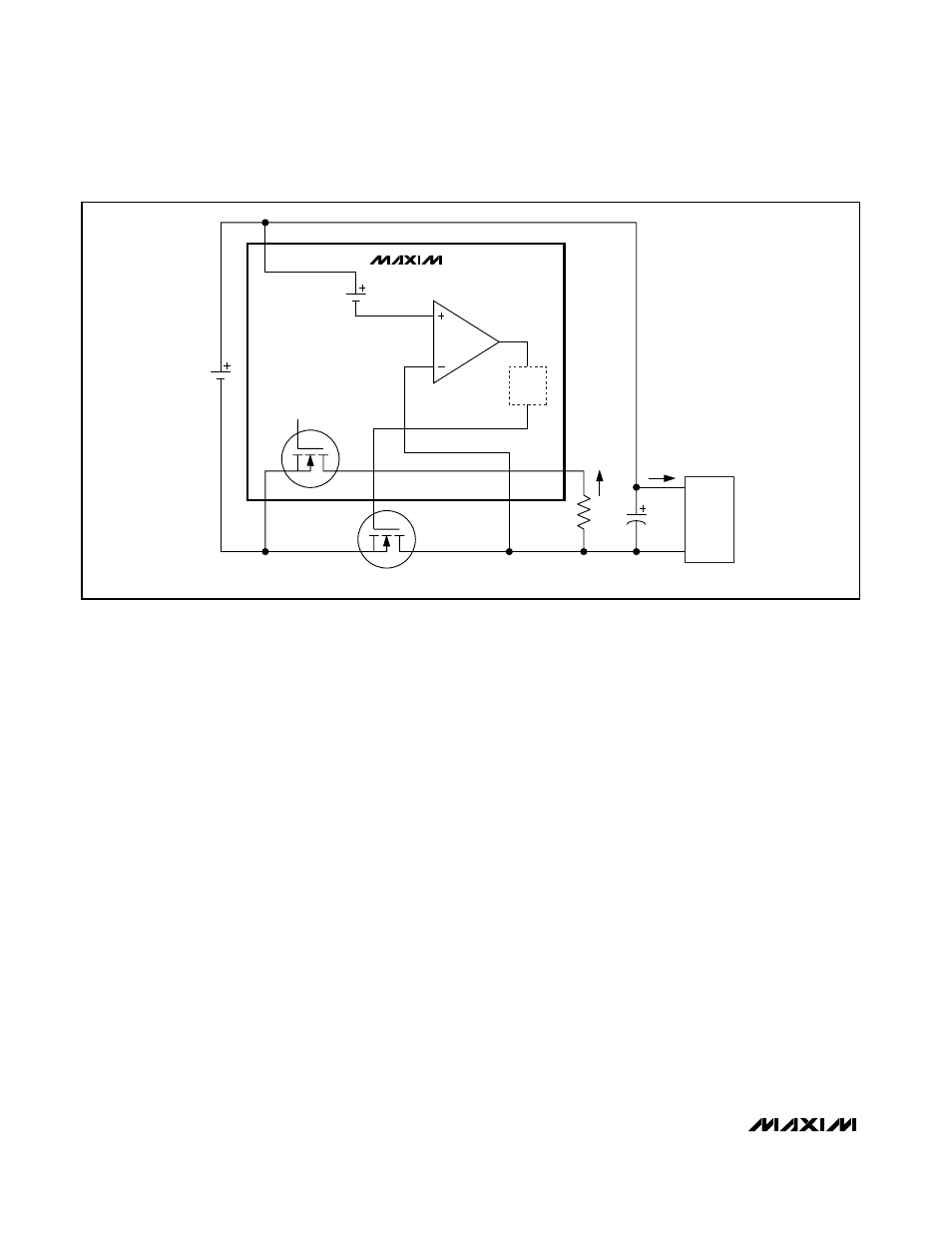
Figure 14. Load Probe Functional Diagram
TIMING
LOGIC
MAX5936
MAX5937
C
LOAD
LOAD
LOAD
OK
V
IN
V
EE
Q1
R
ON
GATE
V
OUT
R
LP
I
TEST
I
LOAD
200mV
GND