Step immunity and no r, Sense, Applications information – Rainbow Electronics MAX5937 User Manual
Page 13
MAX5936/MAX5937
-48V Hot-Swap Controllers with V
IN
Step Immunity and No R
SENSE
______________________________________________________________________________________
13
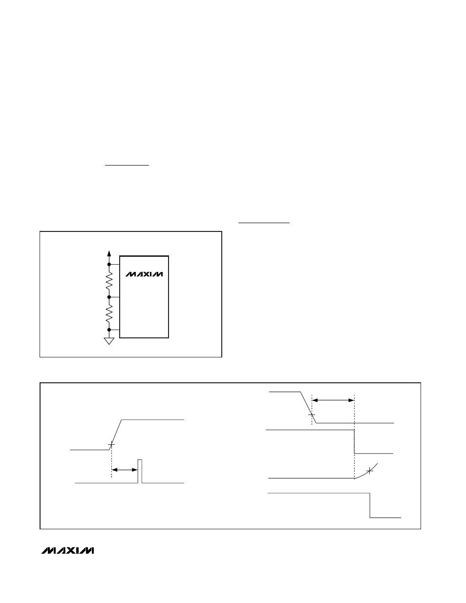
This startup delay is from a valid UVLO condition until the
start of the load-probe test. There is glitch rejection on
UVLO going low, which requires that V
UVLO
remains
below its falling threshold for 1.5ms to turn off the part
(Figure 12b). Use the following formula to calculate the
MAX5936/MAX59337 turn-on voltage:
Where V
ON
is the desired turn-on voltage of the
MAX5936/MAX5937 and V
UVLO_REF,R
is the 1.25V
UVLO rising threshold.
Output Voltage (V
OUT
)
Slew-Rate Control
The V
OUT
slew rate controls the inrush current required
to charge the load capacitor. The MAX5936/MAX5937
have a default internal slew rate set for 9V/ms. The inter-
nal circuit establishing this slew rate accommodates up
to about 1000pF of reverse transfer capacitance (miller
capacitance) in the external power MOSFET without
effecting the default slew rate. Using the default slew
rate, the inrush current required to charge the load
capacitance is given by:
I
INRUSH
(mA) = C
LOAD
(µF) x SR (V/ms)
where SR = 9V/ms (default, typ).
Applications Information
Selecting Resistor and Capacitor
for Step Monitor
When a positive V
IN
step or ramp occurs, the V
IN
increase results in a voltage rise at both STEP_MON
and V
OUT
relative to V
EE
. When the voltage at
STEP_MON is above STEP
TH
the MAX5936/MAX5937
block short-circuit and circuit-breaker faults. During this
STEP_MON high condition, if V
OUT
rises above V
SC
, the
MAX5936/MAX5937 immediately and very rapidly pull
GATE to V
EE
. This turns off the power MOSFET to avoid
inrush current spiking. GATE is held low for 350µs.
About 1ms after the start of GATE pulldown, the
MAX5936/MAX5937 begin to ramp GATE up to turn on
the MOSFET in a controlled manner, which results in
ramping V
OUT
down to the new supply level (see the
GATE Cycles section in Appendix A).
R2
V
V
R1
ON
UVLO_REF, R
=
−
×
1
Figure 11. Setting the MAX5936/MAX5937 Turn-On Voltage
MAX5936
MAX5937
GND
UVLO
V
EE
V
IN
= (GND - V
EE
)
R2
R1
Figure 12. UVLO Timing Diagram
1.3ms
V
SC
V
UVLO_REF,F
UVLO
GATE
V
OUT
PGOOD
UVLO
I
SC_DET
160ms
LOAD PROBE
DETECTION TEST
BEGINS
(a)
(b)
V
UVLO_REF,R