Pin description, Typical operating characteristics (continued) – Rainbow Electronics MAX4399 User Manual
Page 8
MAX4399
Audio/Video Switch for Three SCART
Connectors
8
_______________________________________________________________________________________
Pin Description
PIN
NAME
FUNCTION
1
V_DIG
Digital Supply Voltage. Connect to 5V.
2
DEV_ADDR
Device Address Set Input. Connect to G_DIG to set write and read addresses of 94h and 95h,
respectively. Connect to V_DIG to set write and read addresses of 96h and 97h, respectively.
3
SDA
Bidirectional Data I/O. I
2
C-compatible, 2-wire interface data input/output. Output is open drain.
4
SCL
Clock Input. I
2
C-compatible, 2-wire interface clock.
5
INTERRUPT_OUT
Interrupt Output. INTERRUPT_OUT is an open-drain output that goes high impedance to
indicate a change in the slow switch lines, AUX_SS, TV_SS, or VCR_SS.
6
G_DIG
Digital Ground
7
ENC_L_IN
Digital Encoder Left-Channel Audio Input
8
ST_AUX_IN
Satellite Dish Tone Input
9
ENC_R_IN
Digital Encoder Right-Channel Audio Input
10
AUD_BIAS
Audio Input Bias Voltage. Bypass AUD_BIAS with a 10µF capacitor and a 0.1µF capacitor to
G_AUD.
11, 22, 30
V_AUD
Audio Supply Voltage. Connect all V_AUD together. An on-board linear regulator creates the
+8V audio supply voltage from V12. Bypass pin 30 with a 10µF aluminum electrolytic capacitor
in parallel with a 0.47µF low-ESR ceramic capacitor to audio ground, and bypass pins 11 and
22 with 0.1µF capacitors to audio ground.
12
AUX_L_IN
AUX SCART Left-Channel Audio Input
13
AUX_R_IN
AUX SCART Right-Channel Audio Input
14
VCR_R_IN
VCR SCART Right-Channel Audio Input
15
VCR_L_IN
VCR SCART Left-Channel Audio Input
16
TV_R_IN
TV SCART Right-Channel Audio Input
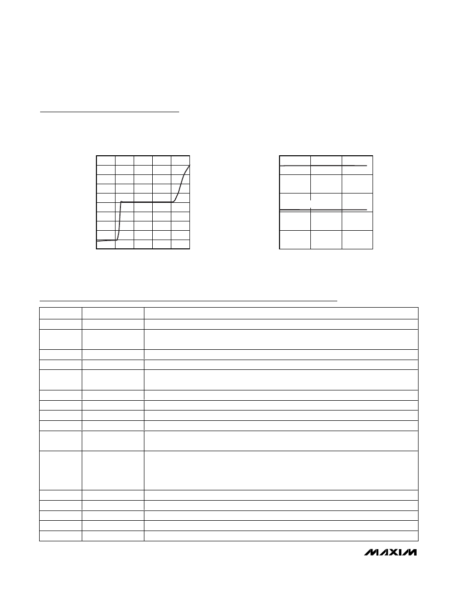
Typical Operating Characteristics (continued)
(V
V12
= 12V, V
V_VID
= 5V, V
V_DIG
= 5V, 0.47µF ceramic X5R capacitor in parallel with a 10µF aluminum electrolytic capacitor from
V_AUD to G_AUD, no load, T
A
= +25°C, unless otherwise noted.)
INPUT CLAMP CURRENT
vs. INPUT VOLTAGE
MAX4399 toc19
INPUT VOLTAGE (V)
INPUT CLAMP CURRENT (mA)
4
3
2
1
-0.4
-0.3
-0.2
-0.1
0
0.1
0.2
0.3
0.4
0.5
-0.5
0
5
OUTPUT BIAS VOLTAGE
vs. TEMPERATURE
MAX4399 toc20
TEMPERATURE (
°C)
OUTPUT BIAS VOLTAGE (V)
50
25
0.5
1.0
1.5
2.0
2.5
0
0
75
RGB, LUMA, CVBS
CHROMA