Absolute maximum ratings, Electrical characteristics – Rainbow Electronics MAX4399 User Manual
Page 2
MAX4399
Audio/Video Switch for Three SCART
Connectors
2
_______________________________________________________________________________________
ABSOLUTE MAXIMUM RATINGS
Stresses beyond those listed under “Absolute Maximum Ratings” may cause permanent damage to the device. These are stress ratings only, and functional
operation of the device at these or any other conditions beyond those indicated in the operational sections of the specifications is not implied. Exposure to
absolute maximum rating conditions for extended periods may affect device reliability.
Voltages
V_VID to G_VID .....................................................-0.3V to +6V
V12 to G_AUD .....................................................-0.3V to +14V
V_DIG to G_DIG ....................................................-0.3V to +6V
G_AUD to G_DIG ...............................................-0.1V to +0.1V
G_VID to G_DIG .................................................-0.1V to +0.1V
G_AUD to G_VID ................................................-0.1V to +0.1V
Video Inputs, Video Outputs, ENC_FS_IN, VCR_FS_IN,
VID_BIAS, TRAP ................................-0.3V to (V
V_VID
+ 0.3V)
V_AUD to G_AUD................................................-0.3V to +9V
Audio Inputs, Audio Outputs,
AUD_BIAS........................................-0.3V to (V
V_AUD
+ 0.3V)
SDA, SCL, DEV_ADDR, INTERRUPT_OUT .........-0.3V to +6V
AUX_SS, TV_SS, VCR_SS ....................-0.3V to (V
V12
+ 0.3V)
Currents
INTERRUPT_OUT ..........................................................+50mA
TRAP................................................................................±4mA
Output Short Circuit
Video Outputs and TV_FS_OUT to V_VID,
V_DIG, G_AUD, G_VID, or G_DIG ........................Continuous
Audio Outputs to V_AUD, V_VID, V_DIG,
G_AUD, G_VID, or G_DIG.....................................Continuous
AUX_SS, TV_SS, and VCR_SS to V12,
V_AUD, V_VID, V_DIG, G_AUD,
G_VID, or G_DIG...................................................Continuous
Continuous Power Dissipation (T
A
= +70°C)
68-Pin Thin QFN (derate 41.7mW/°C
above +70°C).........................................................3333.3mW
Operating Temperature Range...............................0°C to +70°C
Junction Temperature ......................................................+150°C
Storage Temperature Range .............................-65°C to +150°C
Lead Temperature (soldering, 10s) .................................+300°C
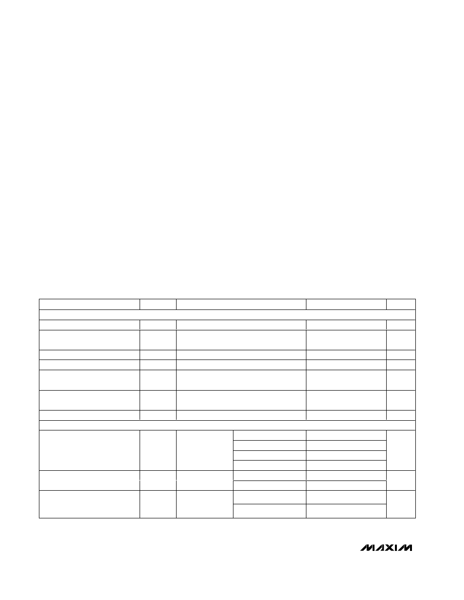
ELECTRICAL CHARACTERISTICS
(V
V12
= 12V, V
V_VID
= 5V, V
V_DIG
= 5V, 0.47µF X5R capacitor in parallel with a 10µF aluminum electrolytic capacitor from V_AUD to
G_AUD, no load, T
A
= 0°C to +70°C, unless otherwise noted. Typical values are at T
A
= +25°C.) (Note 1)
PARAMETER
SYMBOL
CONDITIONS
MIN
TYP
MAX
UNITS
DC
V12 Supply Voltage Range
Inferred from the slow switch output levels
11.4
12
12.6
V
V_VID Supply Voltage Range
Inferred from the output swing of the video
outputs
4.75
5
5.25
V
V_DIG Supply Voltage Range
4.75
5
5.25
V
V12 Quiescent Supply Current
17
35
mA
V_VID Quiescent Supply Current
All video output amplifiers are enabled, no
load
51
116
mA
V_VID Standby Supply Current
All video output amplifiers are in shutdown,
and TV_FS_OUT driver is in shutdown
19
34
mA
V_DIG Quiescent Supply Current
1
3
mA
VIDEO
CVBS and S-VHS
5.5
6
6.5
R, G, B, gain = 5dB
4.5
5
5.5
R, G, B, gain = 6dB
5.5
6
6.5
Voltage Gain
1V
P-P
input
R, G, B, gain = 7dB
6.5
7
7.5
dB
CVBS and S-VHS
110
Small-Signal Bandwidth, -3dB
100mV
P-P
input,
gain = 6dB
R, G, B
110
MHz
CVBS and S-VHS
15
27
Large-Signal Bandwidth, -3dB
1V
P-P
input, gain
= 6dB, T
A
=
+25
°C (Note 2)
R, G, B
30
MHz