Rainbow Electronics MAX4399 User Manual
Page 21
To better protect the MAX4399 against excessive volt-
ages during the cable discharge event, additional 75
Ω
resistors should be placed in series with all inputs and
outputs that go to the SCART connector (
Figure
10).
For harsh environments needing ±15kV protection, the
MAX4385E and MAX4386E single and quad high-
speed op amps feature the industry’s first integrated
±15kV ESD protection on video inputs and outputs.
Power Supplies and Bypassing
The MAX4399 features single +5V and +12V supply
operation, and requires no negative supply. The +12V
supply provides voltage for SCART function switching,
and provides power for the internally generated audio
supply, V_AUD. Place all bypass capacitors as close
as possible to the MAX4399. Bypass V12 to ground
with a 10µF capacitor in parallel with a 0.1µF ceramic
capacitor. Connect all V_AUD pins together and
bypass pin 30 with a 10µF electrolytic capacitor in par-
allel with a 0.47µF low-ESR ceramic capacitor to audio
ground. Bypass V_AUD pins 11 and 22 each with a
0.1µF capacitor to audio ground. Bypass AUD_BIAS to
audio ground with a 10µF electrolytic in parallel with a
0.1µF ceramic capacitor.
Bypass V_DIG with a 0.1µF ceramic capacitor to digital
ground. Bypass each V_VID to video ground with a
0.01µF ceramic capacitor. Connect V_VID in series with
a 200nH ferrite bead to the +5V supply. Bypass the
internally generated video bias, VID_BIAS with a 0.1µF
low-ESR ceramic capacitor to G_VID.
Layout and Grounding
For optimal performance, use controlled-impedance
traces for video signal paths, and place input termina-
tion resistors and output back-termination resistors
close to the MAX4399. Avoid running video traces par-
allel to high-speed data lines.
The MAX4399 provides separate ground connections for
video, audio, and digital supplies. For best performance
use separate ground planes for each of the ground
returns, and connect all three ground planes together at a
single point. Refer to the MAX4399 evaluation kit for a
proven circuit board layout example.
MAX4399
Audio/Video Switch for Three SCART
Connectors
______________________________________________________________________________________
21
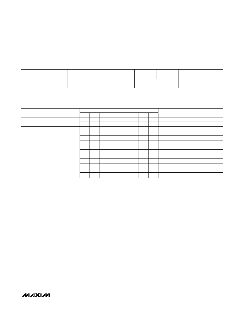
Read Mode: Output Data Format
Table 4. Read Mode Output Data Format
REGISTER
ADDRESS
BIT 7
BIT 6
BIT 5
BIT 4
BIT 3
BIT 2
BIT 1
BIT 0
0Eh
Not used
Power-on
reset
AUX slow switch status
VCR slow switch status
TV slow switch status
Write Mode: Description of Registers
Table 5. Register 00h: Audio Control
BIT
DESCRIPTION
7
6
5
4
3
2
1
0
COMMENTS
—
—
—
—
—
—
—
0
Off
TV Audio Mute
—
—
—
—
—
—
—
1
On (power-on default)
—
—
0
0
0
0
0
—
+6dB gain
—
—
0
0
0
0
1
—
+4dB gain
—
—
0
0
0
1
0
—
+2dB gain
—
—
0
0
0
1
1
—
0dB gain (power-on default)
—
—
0
0
1
0
0
—
-2dB gain
—
—
0
0
1
0
1
—
-4dB gain
—
—
—
—
—
—
—
—
—
—
—
1
1
1
1
0
—
-54dB gain
Volume Control
—
—
1
1
1
1
1
—
-56dB gain
—
0
—
—
—
—
—
—
Off
Zero-Crossing Detector
—
1
—
—
—
—
—
—
On (power-on default)