Rainbow Electronics MAX17031 User Manual
Page 2
MAX17031
Dual Quick-PWM Step-Down Controller with Low-
Power LDO and RTC Regulator for MAIN Supplies
2
_______________________________________________________________________________________
ABSOLUTE MAXIMUM RATINGS
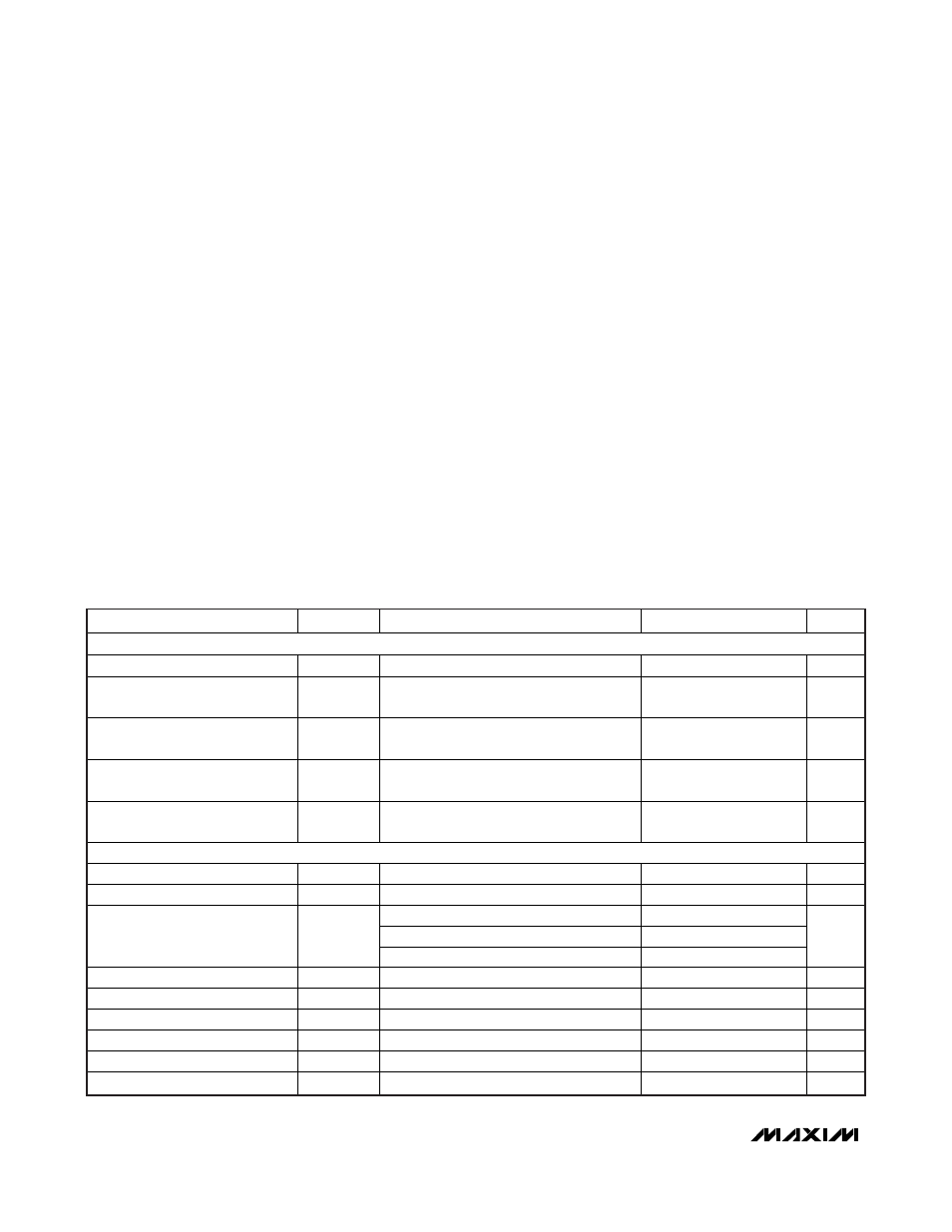
ELECTRICAL CHARACTERISTICS
(Circuit of Figure 2, no load on LDO5, RTC, OUT1, OUT2, and REF, V
IN
= 12V, V
DD
= V
CC
= V
SKIP
= 5V, ONLDO = RTC, ON1 = ON2
= V
CC
, T
A
= 0°C to +85°C, unless otherwise noted. Typical values are at T
A
= +25°C.)
Stresses beyond those listed under “Absolute Maximum Ratings” may cause permanent damage to the device. These are stress ratings only, and functional
operation of the device at these or any other conditions beyond those indicated in the operational sections of the specifications is not implied. Exposure to
absolute maximum rating conditions for extended periods may affect device reliability.
IN to GND ...............................................................-0.3V to +28V
V
DD
, V
CC
to GND .....................................................-0.3V to +6V
RTC, LDO5, ONLDO to GND ...................................-0.3V to +6V
OUT2 to GND ...........................................................-0.3V to +6V
ON1, ON2, PGOOD to GND.....................................-0.3V to +6V
OUT1 to GND..........................................-0.3V to (V
LDO5
+ 0.3V)
SKIP to GND...............................................-0.3V to (V
CC
+ 0.3V)
REF, ILIM1, ILIM2 to GND ..........................-0.3V to (V
CC
+ 0.3V)
DL_ to GND ................................................-0.3V to (V
DD
+ 0.3V)
BST_ to GND ..........................................................-0.3V to +36V
BST_ to V
DD
............................................................-0.3V to +30V
DH1 to LX1 ..............................................-0.3V to (V
BST1
+ 0.3V)
BST1 to LX1..............................................................-0.3V to +6V
DH2 to LX2 ..............................................-0.3V to (V
BST2
+ 0.3V)
BST2 to LX2..............................................................-0.3V to +6V
LDO5, RTC, REF Short Circuit to GND.......................Momentary
RTC Current Continuous.....................................................+5mA
LDO5 Current (Internal Regulator) Continuous ..............+100mA
LDO5 Current (Switched Over) Continuous ...................+200mA
Continuous Power Dissipation (T
A
= +70°C)
24-Pin, 4mm x 4mm Thin QFN (T2444-3)
(derate 27.8mW/°C above +70°C) .................................2.22W
Operating Temperature Range ...........................-40°C to +85°C
Junction Temperature ......................................................+150°C
Storage Temperature Range .............................-65°C to +150°C
Lead Temperature (soldering, 10s) .................................+300°C
PARAMETER
SYMBOL
CONDITIONS
MIN
TYP
MAX
UNITS
INPUT SUPPLIES
IN Input Voltage Range
LDO5 in regulation
6
24
V
IN Standby Supply Current
V
IN
= 6V to 24V, ON1 = ON2 = GND,
ONLDO = RTC
85
175
µA
IN Shutdown Supply Current
V
IN
= 4.5V to 24V,
ON1 = ON2 = ONLDO = GND
40
70 µA
IN Supply Current
I
IN
ON1 = ON2 = V
CC
, V
SKIP
= V
CC
;
V
OUT1
= 5.3V, V
OUT2
= 3.5V
0.1
0.2
mA
V
CC
Bias Supply Current
I
VCC
ON1 = ON2 = V
CC
, V
SKIP
= V
CC
;
V
OUT1
= 5.3V, V
OUT2
= 3.5V
0.7
1.5
mA
PWM CONTROLLERS
OUT1 Output-Voltage Accuracy
V
OUT1
V
SKIP
= 1.8V
4.95
5.00
5.05
V
OUT2 Output-Voltage Accuracy
V
OUT2
V
SKIP
= 1.8V
3.267
3.30
3.333
V
Either SMPS, V
SKIP
= 1.8V, I
LOAD
= 0 to 5A
-0.1
Either SMPS, V
SKIP
= GND, I
LOAD
= 0 to 5A
-1.7
Load Regulation Error
Either SMPS, V
SKIP
= V
CC
, I
LOAD
= 0 to 5A
-1.5
%
Line Regulation Error
Either SMPS, IN = 6V to 28V
0.005
%/V
DH1 On-Time
t
ON1
V
OUT1
= 5.0V (Note 1)
895
1052
1209
ns
DH2 On-Time
t
ON2
V
OUT2
= 3.3V (Note 1)
833
925
1017
ns
Minimum Off-Time
t
OFF(MIN)
(Note 1)
300
400
ns
Soft-Start Slew Rate
t
SS
Rising/falling edge on ON1 or ON2
1
ms
Ultrasonic Operating Frequency
f
SW(USONIC)
V
SKIP
= GND
20
34
kHz
Note: Measurements are valid using a 20MHz bandwidth limit.