Application hints – Rainbow Electronics ADC12L038 User Manual
Page 31
Application Hints
(Continued)
ple operating with a resolution of 12 Bitsasign a 5 MHz
clock frequency and maximum acquistion time of 34 conver-
sion clock periods the ADC’s analog inputs can handle a
source impedance as high as 6 kX The acquisition time
may also be extended to compensate for the settling or
response time of external circuitry connected between the
MUXOUT and A DIN pins
The acquisition time (t
A
) is started by a falling edge of SCLK
and ended by a rising edge of CCLK (see Timing Diagrams)
If SCLK and CCLK are asynchronous one extra CCLK clock
period may be inserted into the programmed acquisition
time for synchronization
Therefore with asnychronous
SCLK and CCLK the acquisition time will change from con-
version to conversion
7 0 INPUT BYPASS CAPACITANCE
External capacitors (0 01 mF – 0 1 mF) can be connected be-
tween the analog input pins CH0 – CH7 and analog ground
to filter any noise caused by inductive pickup associated
with long input leads These capacitors will not degrade the
conversion accuracy
8 0 NOISE
The leads to each of the analog multiplexer input pins
should be kept as short as possible This will minimize input
noise and clock frequency coupling that can cause conver-
sion errors Input filtering can be used to reduce the effects
of the noise sources
9 0 POWER SUPPLIES
Noise spikes on the V
A
a
and V
D
a
supply lines can cause
conversion errors the comparator will respond to the noise
The ADC is especially sensitive to any power supply spikes
that occur during the auto-zero or linearity correction The
minimum power supply bypassing capacitors recommended
are low inductance tantalum capacitors of 10 mF or greater
paralleled with 0 1 mF monolithic ceramic capacitors More
or different bypassing may be necessary depending on the
overall system requirements Separate bypass capacitors
should be used for the V
A
a
and V
D
a
supplies and placed
as close as possible to these pins
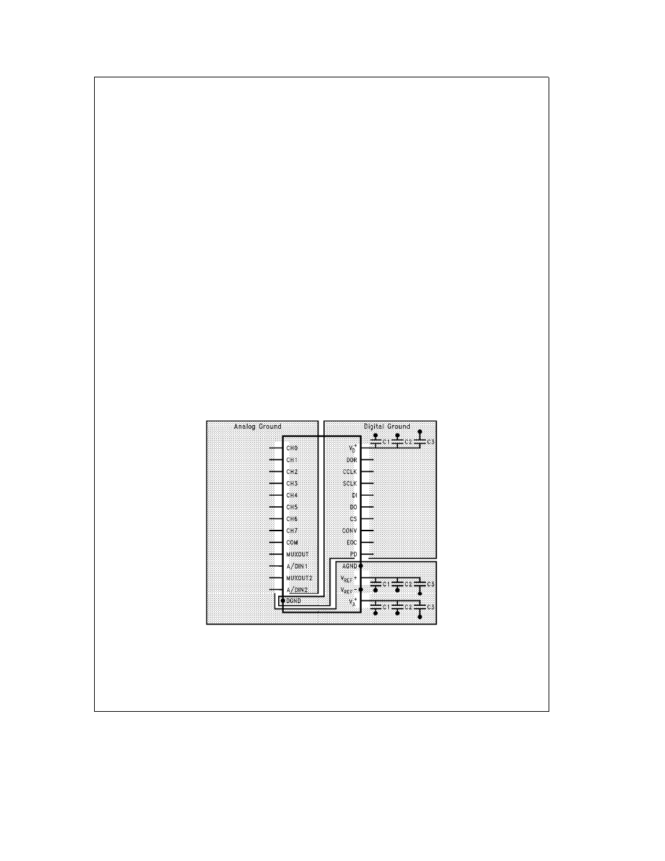
10 0 GROUNDING
The ADC12L030 2 4 8’s performance can be maximized
through proper grounding techniques These include the
use of separate analog and digital ground planes The digi-
tal ground plane is placed under all components that handle
digital signals while the analog ground plane is placed un-
der all components that handle analog signals The digital
and analog ground planes are connected together at only
one point either the power supply ground or at the pins of
the ADC This greatly reduces the occurence of ground
loops and noise
Shown in
Figure 14
is the ideal ground plane layout for the
ADC12L038 along with ideal placement of the bypass ca-
pacitors The circuit board layout shown in
Figure 14
uses
three bypass capacitors 0 01 mF (C1) and 0 1 mF (C2) sur-
face mount capacitors and 10 mF (C3) tantalum capacitor
11 0 CLOCK SIGNAL LINE ISOLATION
The ADC12L030 2 4 8’s performance is optimized by rout-
ing the analog input output and reference signal conductors
as far as possible from the conductors that carry the clock
signals to the CCLK and SCLK pins Ground traces parallel
to the clock signal traces can be used on printed circuit
boards to reduce clock signal interference on the analog
input output pins
TL H 11830 – 44
FIGURE 14 Ideal Ground Plane for the ADC12L038
31