Application hints – Rainbow Electronics ADC12L038 User Manual
Page 30
Application Hints
(Continued)
system reference stability requirements because the analog
input voltage and the ADC reference voltage move togeth-
er This maintains the same output code for given input con-
ditions For absolute accuracy where the analog input volt-
age varies between very specific voltage limits a time and
temperature stable voltage source can be connected to the
reference inputs Typically the reference voltage’s magni-
tude will require an initial adjustment to null reference volt-
age induced full-scale errors
Below are recommended references along with some key
specifications
Output
Temperature
Part Number
Voltage
Coefficient
Tolerance
(max)
LM4041CIM3-Adj
g
0 5%
g
100ppm C
LM4040AIM3-2 5
g
0 1%
g
100ppm C
LM9140BYZ-2 5
g
0 5%
g
25ppm C
LM368Y-2 5
g
0 1%
g
20ppm C
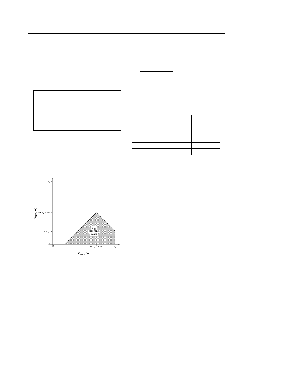
The reference voltage inputs are not fully differential The
ADC12L030 2 4 8 will not generate correct conversions or
comparisons if V
REF
a
is taken below V
REF
b
Correct con-
versions result when V
REF
a
and V
REF
b
differ by 1V and
remain at all times between ground and V
A
a
The V
REF
common mode range (V
REF
a
a
V
REF
b
) 2 is restricted to
(0 1
c
V
A
a
) to (0 6
c
V
A
a
) Therefore with V
A
a
e
3 3V
the center of the reference ladder should not go below
0 33V or above 1 98V
Figure 13
is a graphic representation
of the voltage restrictions on V
REF
a
and V
REF
b
TL H 11830 – 43
FIGURE 13 V
REF
Operating Range
4 0 ANALOG INPUT VOLTAGE RANGE
The ADC12L030 2 4 8’s fully differential ADC generate a
two’s complement output that is found by using the equa-
tions shown below
for (12-bit) resolution the Output Code e
(V
IN
a
b
V
IN
b
) (4096)
(V
REF
a
b
V
REF
b
)
for (8-bit) resolution the Output Code e
(V
IN
a
b
V
IN
b
) (256)
(V
REF
a
b
V
REF
b
)
Round off to the nearest integer value between b4096 to
4095 for 12-bit resolution and between b256 to 255 for 8-
bit resolution if the result of the above equation is not a
whole number
Examples are shown in the table below
Digital
V
REF
a
V
REF
b
V
IN
a
V
IN
b
Output
Code
a
2 5V
a
1V
a
1 5V
0V
0 1111 1111 1111
a
2 500V
0V
a
2V
0V
0 1100 1100 1101
a
2 500V
0V
a
2 499V a2 500V 1 1111 1111 1111
a
2 500V
0V
0V
a
2 500V 1 0000 0000 0000
5 0 INPUT CURRENT
At the start of the acquisition window (t
A
) a charging current
flows into or out of the analog input pins (A DIN1 and
A DIN2) depending on the input voltage polarity The ana-
log input pins are CH0 – CH7 and COM when A DIN1 is tied
to MUXOUT1 and A DIN2 is tied to MUXOUT2 The peak
value of this input current will depend on the actual input
voltage applied the source impedance and the internal mul-
tiplexer switch on resistance
With MUXOUT1 tied to
A DIN1 and MUXOUT2 tied to A DIN2 the internal multi-
plexer switch on resistance is typically 1 6 kX The A DIN1
and A DIN2 mux on resistance is typically 750X
6 0 INPUT SOURCE RESISTANCE
For low impedance voltage sources (
k
600X) the input
charging current will decay before the end of the S H’s
acquisition time of 2 ms (10 CCLK periods with f
C
e
5 MHz)
to a value that will not introduce any conversion errors For
high source impedances the S H’s acquisition time can be
increased to 18 or 34 CCLK periods For less ADC resolu-
tion and or slower CCLK frequencies the S H’s acquisition
time may be decreased to 6 CCLK periods To determine
the number of clock periods (N
c
) required for the acquisition
time with a specific source impedance for the various reso-
lutions the following equations can be used
12 Bit a Sign
N
C
e
R
S
a
2 3
c
f
C
c
0 824
8 Bit a Sign
N
C
e
R
S
a
2 3
c
f
C
c
0 57
Where f
C
is the conversion clock (CCLK) frequency in MHz
and R
S
is the external source resistance in kX As an exam-
30