Application hints – Rainbow Electronics ADC12L038 User Manual
Page 26
Application Hints
(Continued)
sary to be input to the ADC to accomplish this configuration
modification The next instruction shown in
Figure 6
issued
to the A D starts conversion Na1 with 8 bits of resolution
formatted MSB first Again the data output during this I O
cycle is the data from conversion N
The number of SCLKs applied to the A D during any con-
version I O sequence should vary in accord with the data
out word format chosen during the previous conversion I O
sequence The various formats and resolutions available
are shown in Table I In
Figure 6
since 8-bit without sign
MSB first format was chosen during I O sequence 4 the
number of SCLKs required during I O sequence 5 is 8 In
the following I O sequence the format changes to 12-bit
without sine MSB first therefore the number of SCLKs re-
quired during I O sequence 6 changes accordingly to 12
1 3 CS Low Continuously Considerations
When CS is continuously low it is important to transmit the
exact number of SCLK pulses that the ADC expects Not
doing so will desynchronize the serial communications to
the ADC When the supply power is first applied to the ADC
it will expect to see 13 SCLK pulses for each I O transmis-
sion The number of SCLK pulses that the ADC expects to
see is the same as the digital output word length The digital
output word length is controlled by the Data Out (DO) for-
mat The DO format maybe changed any time a conversion
is started or when the sign bit is turned on or off The table
below details out the number of clock periods required for
different DO formats
Number of
DO Format
SCLKs
Expected
8-Bit MSB or LSB First
SIGN OFF
8
SIGN ON
9
12-Bit MSB or LSB First
SIGN OFF
12
SIGN ON
13
16-Bit MSB or LSB first
SIGN OFF
16
SIGN ON
17
If erroneous SCLK pulses desynchronize the communica-
tions the simplest way to recover is by cycling the power
supply to the device Not being able to easily resynchronize
the device is a shortcoming of leaving CS low continuously
The number of clock pulses required for an I O exchange
may be different for the case when CS is left low continu-
ously vs the case when CS is cycled Take the I O se-
quence detailed in
Figure 5
(Typical Power Supply Se-
quence) as an example The table below lists the number of
SCLK pulses required for each instruction
Instruction
CS Low
CS Strobed
Continuously
Auto Cal
13 SCLKs
8 SCLKs
Read Status
13 SCLKs
8 SCLKs
Read Status
13 SCLKs
8 SCLKs
12-Bit a Sign Conv 1
13 SCLKs
8 SCLKs
12-Bit a Sign Conv 2
13 SCLKs
13 SCLKs
1 4 Analog Input Channel Selection
The data input on DI also selects the channel configuration
for a particular A D conversion (see Tables II III IV and V)
In
Figure 6
the only times when the channel configuration
could be modified would be during I O sequences 1 4 5
and 6 Input channels are reselected before the start of
each new conversion Shown below is the data bit stream
required on DI during I O sequence number 4 in
Figure 6
to set CH1 as the positive input and CH0 as the negative
input for the different versions of ADCs
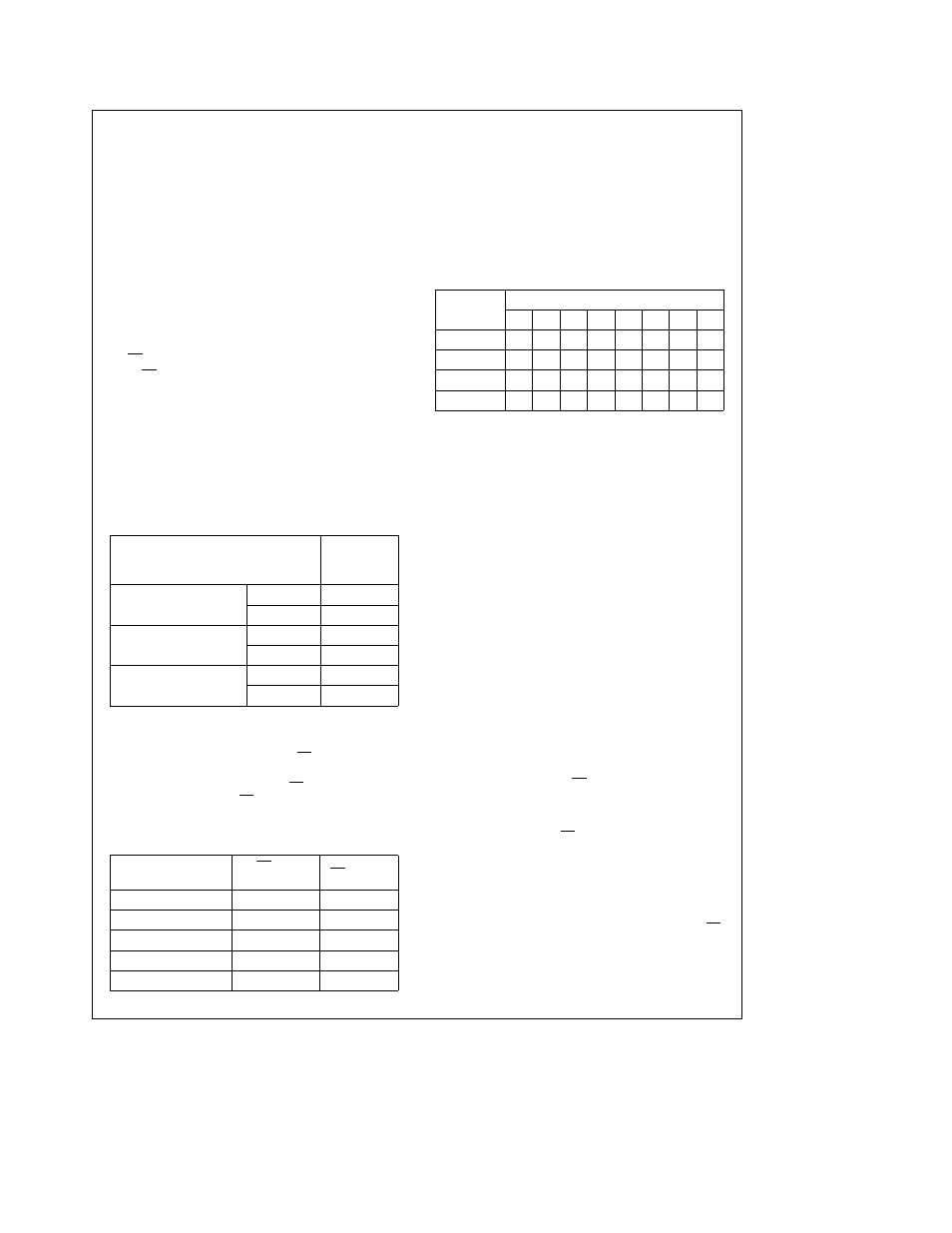
Number
Part
DI Data
DI0
DI1
DI2
DI3
DI4
DI5
DI6
DI7
ADC12L030
L
H
L
L
H
L
X
X
ADC12L032
L
H
L
L
H
L
X
X
ADC12L034
L
H
L
L
L
H
L
X
ADC12L038
L
H
L
L
L
L
H
L
Where X can be a logic high (H) or low (L)
1 5 Power Up Down
The ADC may be powered down at any time by taking the
PD pin HIGH or by the instruction input on DI (see Tables V
and VI and the Power Up Down timing diagrams) When
the ADC is powered down in this way the circuitry necessary
for an A D conversion is deactivated The circuitry neces-
sary for digital I O is kept active Hardware power up down
is controlled by the state of the PD pin Software power up
down is controlled by the instruction issued to the ADC If a
software power up instruction is issued to the ADC while a
hardware power down is in effect (PD pin high) the device
will remain in the power-down state If a software power
down instruction is issued to the ADC while a hardware
power up is in effect (PD pin low) the device will power
down When the device is powered down by software it
may be powered up by either issuing a software power up
instruction or by taking PD pin high and then low If the
power down command is issued during an A D conversion
that conversion is disrupted Therefore the data output after
power up cannot be relied on
1 6 User Mode and Test Mode
An instruction may be issued to the ADC to put it into test
mode Test mode is used by the manufacturer to verify com-
plete functionality of the device During test mode CH0 –
CH7 become active outputs If the device is inadvertently
put into the test mode with CS low continuously the serial
communications may be desynchronized Synchronization
may be regained by cycling the power supply voltage to the
device Cycling the power supply voltage will also set the
device into user mode If CS is used in the serial interface
the ADC may be queried to see what mode it is in This is
done by issuing a ‘‘read STATUS register’’ instruction to the
ADC When bit 9 of the status register is high the ADC is in
test mode when bit 9 is low the ADC is in user mode As an
alternative to cycling the power supply an instruction se-
quence may be used to return the device to user mode This
instruction sequence must be issued to the ADC using CS
26