Application hints – Rainbow Electronics ADC12L038 User Manual
Page 27
Application Hints
(Continued)
The following table lists the instructions required to return
the device to user mode
Instruction
DI Data
DI0 DI1 DI2 DI3 DI4 DI5 DI6 DI7
TEST MODE
H
X
X
X
H
H
H
H
RESET
L
L
L
L
H
H
H
L
TEST MODE
L
L
L
L
H
L
H
L
INSTRUCTIONS
L
L
L
L
H
L
H
H
USER MODE
L
L
L
L
H
H
H
H
Power Up
L
L
L
L
H
L
H
L
Set DO with
H
or without
or
L
L
L
H
H
L
H
Sign
L
Set
H
H
Acquisition
or
or
L
L
H
H
H
L
Time
L
L
Start
H
H
H
H
H
H
H
a
or
or
or
or
L
or
or
or
Conversion
L
L
L
L
L
L
L
X
e
Don’t Care
After returning to user mode with the user mode instruction
the power up data with or without sign and acquisition time
instructions need to be resent to ensure that the ADC is in
the required state before a conversion is started
1 7 Reading the Data Without Starting a Conversion
The data from a particular conversion may be accessed
without starting a new conversion by ensuring that the
CONV line is taken high during the I O sequence See the
Read Data timing diagrams Table VI describes the opera-
tion of the CONV pin
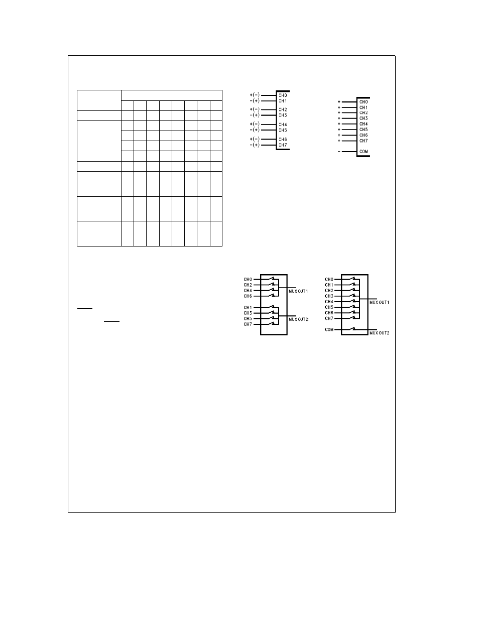
2 0 DESCRIPTION OF THE ANALOG MULTIPLEXER
For the ADC12L038 the analog input multiplexer can be
configured with 4 differential channels or 8 single ended
channels with the COM input as the zero reference or any
combination thereof (see
Figure 7
) The difference between
the voltages on the V
REF
a
and V
REF
b
pins determines the
input voltage span (V
REF
) The analog input voltage range is
0 to V
A
a
Negative digital output codes result when V
IN
b
l
V
IN
a
The actual voltage at V
IN
b
or V
IN
a
cannot go below
AGND
4 Differential
8 Single-Ended Channels
Channels
with COM
as Zero Reference
TL H 11830 – 38
TL H 11830 – 39
FIGURE 7
CH0 CH2 CH4 and CH6 can be assigned to the MUX-
OUT1 pin in the differential configuration while CH1 CH3
CH5 and CH7 can be assigned to the MUXOUT2 pin In the
differential configuration the analog inputs are paired as fol-
lows CH0 with CH1 CH2 with CH3 CH4 with CH5 and CH6
with CH7 The A DIN1 and A DIN2 pins can be assigned
positive or negative polarity
With
the
single-ended
multiplexer
configuration
CH0
through CH7 can be assigned to the MUXOUT1 pin The
COM pin is always assigned to the MUXOUT2 pin A DIN1
is assigned as the positive input A DIN2 is assigned as the
negative input (See
Figure 8
)
Differential
Single-Ended
Configuration
Configuration
TL H 11830 – 40
TL H 11830 – 41
A DIN1 and A DIN2 can be as-
A DIN1 is
a
input
signed as the
a
or
b
input
A DIN2 is
b
input
FIGURE 8
The Multiplexer assignment tables for the ADC12L030 2 4 8
(Tables II III and IV) summarize the aforementioned func-
tions for the different versions of A Ds
2 1 Biasing for Various Multiplexer Configurations
Figure 9
is an example of biasing the device for single-end-
ed operation The sign bit is always low The digital output
range is 0 0000 0000 0000 to 0 1111 1111 1111 One LSB
is equal to 610 mV (2 5V 4096 LSBs)
27