Pin descriptions – Rainbow Electronics ADC12L038 User Manual
Page 21
Pin Descriptions
(Continued)
V
REF
a
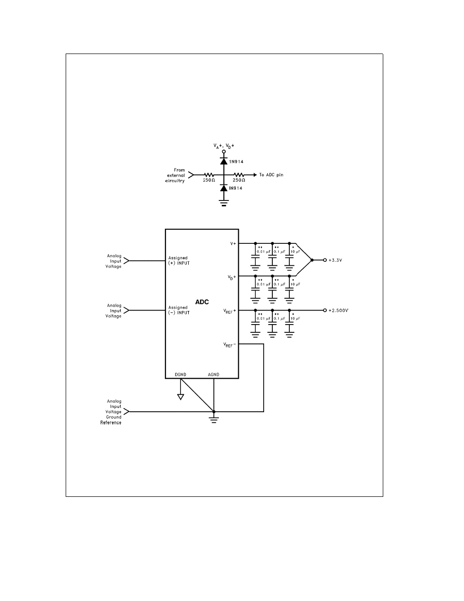
This is the positive analog voltage reference in-
put In order to maintain accuracy the voltage
range of V
REF
(V
REF
e
V
REF
a
b
V
REF
b
) is
1 V
DC
to 3 3 V
DC
and the voltage at V
REF
a
cannot exceed V
A
a
See
Figure 4
for recom-
mended bypassing
V
REF
b
The negative voltage reference input In order
to maintain accuracy the voltage at this pin
must not go below GND or exceed V
A
a
(See
Figure 4
)
V
A
a
V
D
a
These are the analog and digital power supply
pins V
A
a
and V
D
a
are not connected together
on the chip These pins should be tied to the
same power supply and bypassed separately
(see
Figure 4
) The operating voltage range of
V
A
a
and V
D
a
is 3 0 V
DC
to 5 5 V
DC
DGND
This is the digital ground pin (see
Figure 4
)
AGND
This is the analog ground pin (see
Figure 4
)
TL H 11830 – 34
FIGURE 3 Protecting the MUXOUT1 MUXOUT2 A DIN1 and A DIN2 Analog Pins
TL H 11830 – 35
Tantalum
Monolithic Ceramic or better
FIGURE 4 Recommended Power Supply Bypassing and Grounding
21
- MAX5151 (16 pages)
- MAXQ3108 (64 pages)
- MAX5661 (39 pages)
- MAX6691 (7 pages)
- MAX5362 (12 pages)
- ADC10158 (26 pages)
- MAX8922L (14 pages)
- MAX8596Z (8 pages)
- MAX7491 (18 pages)
- MAX15040 (15 pages)
- MAX5177 (16 pages)
- ADC08138 (22 pages)
- MAX5961 (42 pages)
- T89C51RD2 (86 pages)
- MAX16055 (9 pages)
- MAX6659 (17 pages)
- ADC0820 (20 pages)
- MAX6678 (19 pages)
- MAX8884Z (15 pages)
- MAX16915 (9 pages)
- MAX8620 (18 pages)
- MAX5144 (12 pages)
- MAX6670 (8 pages)
- MAX8760 (39 pages)
- W78C32C (14 pages)
- MX7533 (8 pages)
- MAX8727 (13 pages)
- MAX9053 (15 pages)
- W78C54 (16 pages)
- MAX8614B (15 pages)
- W90N740 (219 pages)
- MAX6626 (13 pages)
- ADC10738 (30 pages)
- MAX17000 (31 pages)
- MAX5051 (21 pages)
- MAXQ1004 (18 pages)
- MAX6871 (51 pages)
- MX7847 (12 pages)
- MAX6608 (6 pages)
- MAX17083 (15 pages)
- MAX6641 (17 pages)
- MAX5251 (16 pages)
- MAX6338 (8 pages)
- MAX6690 (16 pages)
- MAX8668 (18 pages)