Pin description – Rainbow Electronics MAX15025 User Manual
Page 9
MAX15024/MAX15025
Single/Dual, 16ns, High Sink/Source
Current Gate Drivers
_______________________________________________________________________________________
9
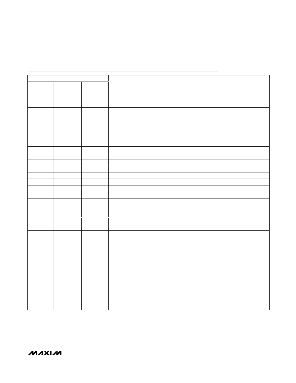
Pin Description
PIN
MAX15024
MAX15025A
MAX15025B
MAX15025E
MAX15025F
MAX15025C
MAX15025D
MAX15025G
MAX15025H
NAME
FUNCTION
1
1
1
FB/SET
LDO Regulator Output Set. Feedback for V
REG
adjustment (V
FB
> 200mV).
Connect FB/SET to GND for a fixed 10V output REG. Connect FB/SET to a
resistor ladder to set V
REG
.
2
2
2
V
CC
Power-Supply Input. Bypass to GND with a low-ESR ceramic capacitor of
1µF. Input of the internal housekeeping regulator and of the main REG
regulator.
3
3
3
GND
Signal Ground
4
—
—
IN+
Driver Noninverting Logic Input. Connect to V
CC
when not used.
—
4
4
IN1
Driver 1 Noninverting Logic Input
5
—
—
IN-
Driver Inverting Logic Input. Connect to GND when not used.
—
5
—
IN2
Driver 2 Noninverting Logic Input
—
—
5
IN2
Driver 2 Inverting Logic Input
6
6
6
PGND
Power Ground. Sink current return. Source of the internal pulldown
n-channel transistor.
7
—
—
N_OUT
Sink Output. Open-drain n-channel output. N_OUT sinks current for power
MOSFET turn-off.
—
7
7
OUT2
Driver 2 Output
8
—
—
P_OUT
Source Output. Pullup p-channel output (open drain). Sources current for
power MOSFET turn-on.
—
8
8
OUT1
Driver 1 Output
9
9
9
DRV
Output Driver Supply Voltage. Decouple DRV with a low ESR > 0.1µF
ceramic capacitor to PGND placed in close proximity to the device. DRV
can be powered independently from REG. Connect DRV, REG, and V
CC
together when there is no need for special DRV supply sequencing and
the power-MOSFET gate voltage does not need to be regulated or limited.
10
10
10
REG
Voltage Regulator Output. Connect to DRV for driving the power MOSFET
with regulated V
GS
amplitude. Bypass with a low-ESR 1µF (minimum)
ceramic capacitor to GND placed in close proximity to the device to
ensure regulator stability.
—
—
—
EP
Exposed Pad. Internally connected to GND. Connect to GND plane or
thermal pad and use multiple vias to a solid copper area on the bottom of
the PCB.