Rainbow Electronics MAX15025 User Manual
Page 2
MAX15024/MAX15025
Single/Dual, 16ns, High Sink/Source
Current Gate Drivers
2
_______________________________________________________________________________________
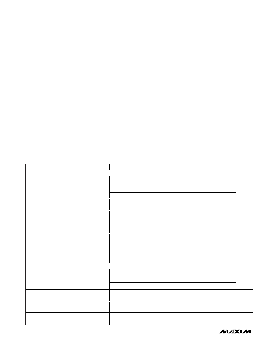
ABSOLUTE MAXIMUM RATINGS
MAX15024 ELECTRICAL CHARACTERISTICS
(V
CC
= V
DRV
= V
REG
= 10V, FB/SET = GND, T
A
= T
J
= -40°C to +125°C, unless otherwise noted. Typical values are at T
A
= T
J
=
+ 25°C). (Note 2)
Stresses beyond those listed under “Absolute Maximum Ratings” may cause permanent damage to the device. These are stress ratings only, and functional
operation of the device at these or any other conditions beyond those indicated in the operational sections of the specifications is not implied. Exposure to
absolute maximum rating conditions for extended periods may affect device reliability.
V
CC
to GND ............................................................-0.3V to +30V
REG to GND ..............-0.3V to the lower of +22V or (V
CC
+ 0.3V)
DRV to PGND .........................................................-0.3V to +22V
IN_ ..........................................................................-0.3V to +22V
FB/SET to GND.........................................................-0.3V to +6V
P_OUT to DRV ........................................................-22V to +0.3V
N_OUT to PGND.....................................................-0.3V to +22V
OUT1, OUT2 to PGND ..............................-0.3V to (V
DRV
+ 0.3V)
PGND to GND .......................................................-0.3V to +0.3V
P_OUT, N_OUT Continuous Source/Sink Current* .......... 200mA
OUT1, OUT2 Continuous Source/Sink Current*................200mA
Continuous Power Dissipation (T
A
= +70°C)
10-Pin TDFN, Single-Layer Board
(derate 18.5mW/°C above +70°C) ...........................1481.5mW
Junction-to-Case Thermal Resistance (Note 1) ..............8.5°C/W
10-Pin TDFN, Multilayer Board
(derate 24.4mW/°C above +70°C) ...........................1951.2mW
Junction-to-Case Thermal Resistance (Note 1) ..............8.5°C/W
Operating Temperature Range .........................-40°C to +125°C
Junction Temperature ......................................................+150°C
Storage Temperature Range .............................-65°C to +150°C
Lead Temperature (soldering, 10s) .................................+300°C
PARAMETER
SYMBOL
CONDITIONS
MIN
TYP
MAX
UNITS
SYSTEM SPECIFICATIONS
MAX15024B/D
6.5
28.0
V
CC
powered only, V
REG
=
V
DRV
decoupled with
minimum 1µF to GND
MAX15024A/C
4.5
28.0
V
CC
= V
REG
= V
DRV
(MAX15024D)
6.5
18.0
Input Voltage Range
V
CC
V
CC
= V
REG
= V
DRV
(MAX15024C)
4.5
18.0
V
V
DRV
Turn-On Voltage
V
DRV
_
ON
V
CC
= V
REG
= 10V, IN+ = V
CC
, IN- = GND
1.7
2.3
V
Quiescent Supply Current
IN_ = V
CC
or GND
700
1350
µA
Quiescent Supply Current
Under UVLO Condition
IN_ = V
CC
or GND
250
µA
Switching Supply Current
Switching at 250kHz, C
L
= 0
1.5
3.0
mA
V
CC
Undervoltage Lockout
UVLO_ V
CC
V
CC
rising
3.0
3.4
3.8
V
V
CC
Undervoltage-Lockout
Hysteresis
300
mV
V
CC
rising
100
V
CC
Undervoltage Lockout to
Output Delay
V
CC
falling
2
µs
REG REGULATOR (V
CC
= 12V, REG = V
DRV
, C
L
= 1µF, FB/SET = GND)
Output Voltage
V
REG
12V < V
CC
< 28V, 0 < I
LOAD
< 10mA
9
10
11
V
V
CC
= 6.5V, I
LOAD
= 100mA
0.4
0.9
Dropout Voltage
V
R
_
DO
V
CC
= 4.5V, I
LOAD
= 50mA
0.2
0.5
V
Load Regulation
V
CC
= 12V, I
LOAD
= 0 to 100mA
1
%
Line Regulation
12V < V
CC
< 28V
10
mV
FB/SET Reference Voltage
External resistive divider connected at
FB/SET
1.10
1.23
1.35
V
FB/SET Threshold
V
FB
falling
220
mV
FB/SET Input Leakage Current
V
FB
= 4.5V (Note 3)
-125
+125
nA
*
Continuous output current is limited by the power dissipation of the package.
Note 1: Package thermal resistances were obtained using the method described in JEDEC specification JESD51-7, using a four-
layer board. For detailed information on package thermal considerations, see
www.maxim-ic.com/thermal.tutorial
.