Rainbow Electronics MAX15025 User Manual
Page 11
Power Dissipation
Power dissipation of the MAX15024/MAX15025 con-
sists of three components: the quiescent current,
capacitive charge and discharge of internal nodes, and
the output current (either capacitive or resistive load).
The sum of these components must be kept below the
maximum power-dissipation limit. The quiescent cur-
rent is 700µA typ. The current required to charge and
discharge the internal nodes is frequency dependent
(see the
Typical Operating Characteristics
). The
MAX15024/MAX15025 power dissipation when driving
a ground-referenced resistive load is:
P = D x R
ON(MAX)
x I
LOAD2
where D is the fraction of the period the MAX15024/
MAX15025s’ output pulls high, R
ON(MAX)
is the maxi-
mum on-resistance of the device with the output high
(p-channel), and I
LOAD
is the output load current of the
MAX15024/MAX15025. For capacitive loads, the power
dissipation for each driver is:
P = C
LOAD
x V
DRV2
x FREQ
where C
LOAD
is the capacitive load, V
DRV
is the driver
supply voltage, and FREQ is the switching frequency.
Layout Information
The MAX15024/MAX15025 MOSFET drivers source and
sink large currents to create very fast rise and fall edges
at the gate of the switching MOSFET. The high di/dt can
cause unacceptable ringing if the trace lengths and
impedances are not well controlled. The following
printed-circuit board (PCB) layout guidelines are recom-
mended when designing with the MAX15024/MAX15025:
• Place one or more 1µF decoupling ceramic capaci-
tor(s) from V
DRV
to PGND as close to the device as
possible. At least one storage capacitor of 10µF (min)
should be located on the PCB with a low resistance
path to the V
CC
pin of the MAX15024/MAX15025.
• There are two AC current loops formed between the
device and the gate of the MOSFET being driven.
The MOSFET looks like a large capacitance from
gate to source when the gate is being pulled low.
The active current loop is from MOSFET gate to
OUT_ of the MAX15024/MAX15025 to PGND of the
MAX15024/MAX15025, and to the source of the
MOSFET. When the gate of the MOSFET is being
pulled high, the active current loop is from the V
DD
terminal of the V
DRV
terminal of decoupling capaci-
tor, to the V
DRV
of the MAX15024/MAX15025, to the
OUT_ of the MAX15024/MAX15025, to the MOSFET
gate, to the MOSFET source, and to the negative ter-
minal of the decoupling capacitor. Both charging
current loop and discharging current loop are impor-
tant. It is important to minimize the physical distance
and the impedance in these AC current paths.
• Keep the device as close as possible to the MOSFET.
• In the multilayer PCB, the inner layers should consist
of a GND plane containing the discharging and
charging current loops.
MAX15024/MAX15025
Single/Dual, 16ns, High Sink/Source
Current Gate Drivers
______________________________________________________________________________________
11
IN+
P_OUT AND
N_OUT CONNECTED
TOGETHER
OR OUT1/OUT2
V
IL
V
IH
t
D-OFF
t
F
90%
10%
t
D-ON
t
R
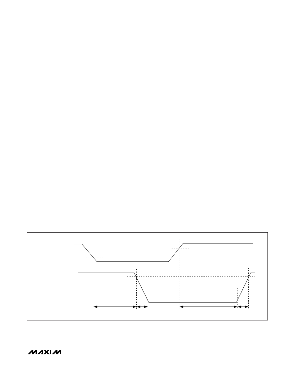
Figure 1. Timing Diagram