Max7311, Table 1. command byte register, Slave address – Rainbow Electronics MAX7311 User Manual
Page 8: Data bus transaction
MAX7311
MAX7311 generates the acknowledge bit since the
MAX7311 is the recipient. When the MAX7311 is trans-
mitting to the master, the master generates the
acknowledge bit.
Slave Address
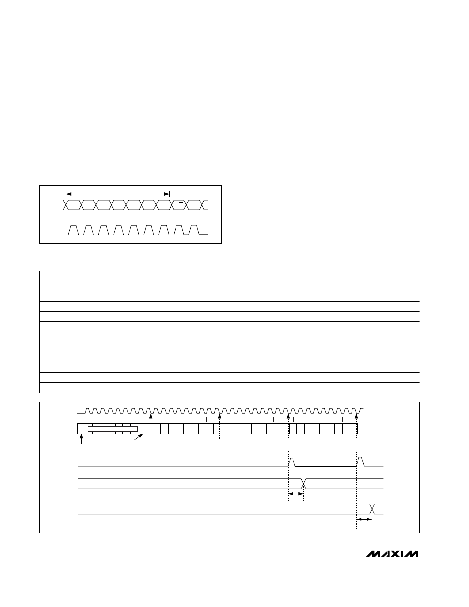
The MAX7311 has a 7-bit-long slave address (Figure 6).
The 8th bit following the 7-bit slave address is the R/W
bit. Set this bit low for a write command and high for a
read command.
Slave address pins AD2, AD1, and AD0 choose 1 of 64
slave ID addresses (Table 7).
Data Bus Transaction
The command byte is the first byte to follow the 8-bit
device slave address during a write transmission
(Table 1, Figure 7). The command byte is used to deter-
mine which of the following registers are written or read.
Writing to Port Registers
Transmit data to the MAX7311 by sending the device
slave address and setting the LSB to a logic zero. The
command byte is sent after the address and deter-
mines which registers receive the data following the
command byte (Figure 7).
2-Wire-Interfaced 16-Bit I/O Port Expander
with Interrupt
8
_______________________________________________________________________________________
SDA
SDA
A6
A5
A4
A3
A2
A1
A0
MSB
LSB
ACK
R/W
PROGRAMMABLE
Figure 6. Slave Address
COMMAND BYTE
ADDRESS (HEX)
FUNCTION
PROTOCOL
POWER-UP
DEFAULT
0x00
Input port 1
Read byte
XXXX XXXX
0x01
Input port 2
Read byte
XXXX XXXX
0x02
Output port 1
Read/write byte
1111 1111
0x03
Output port 2
Read/write byte
1111 1111
0x04
Port 1 polarity inversion
Read/write byte
0000 0000
0x05
Port 2 polarity inversion
Read/write byte
0000 0000
0x06
Port 1 configuration
Read/write byte
1111 1111
0x07
Port 2 configuration
Read/write byte
1111 1111
0x08
Timeout register
Read/write byte
0000 0001
0xFF
Factory reserved. (Do not write to this register.)
—
—
Table 1. Command Byte Register
1
2
3
4
5
6
7
8
9
SCL
SDA
S
A
0
0
0
0
0
0
1
7
6
5
4
3
2
1
0
A
7
6
5
4
3
2
1
0
A
0
A
SLAVE ADDRESS
COMMAND BYTE
PORT 1 DATA
PORT 2 DATA
R/W
ACKNOWLEDGE
FROM SLAVE
ACKNOWLEDGE
FROM SLAVE
START
CONDITION
ACKNOWLEDGE
FROM SLAVE
ACKNOWLEDGE
FROM SLAVE
t
PV
t
PV
WRITE TO PORT
DATA OUT PORT 1
READ FROM PORT 2
Figure 7. Writes to Output Registers Through Write Byte Protocol